
Kelvin probes provide a nondestructive and contact-free method of measuring the work function differences of various material combinations. These probes can have a variety of designs, including different tip shapes, lengths, and radii. To find an optimal design while minimizing the need for extensive testing, one group of researchers used the COMSOL Multiphysics® software. Here’s what they found…
Taking a Closer Look at Kelvin Probes
A Kelvin probe can determine the contact potential difference (or work function difference) of materials. This type of probe, which is based on a time-varying capacitor, works by using two electrodes:
- Movable probe made of a material with a known work function
- Fixed sample made of a material with an unknown work function
When these electrodes are electrically connected, the Fermi levels reach equilibrium. The electrons from the material with the lower work function flow into the material with the higher work function. This flow creates a contact potential difference, charging the capacitor. Additionally, the vibrations in the movable electrode change the electrical energy stored inside the capacitor and create a flowing electrical current. By measuring this current, we can determine the work function difference. It’s also possible to establish a compensated operation and make the current zero by applying an external bias voltage. This approach results in a bias voltage equal to the work function difference between the two electrode materials.
Among other things, Kelvin probes are used for Kelvin probe force microscopy (KPFM), a noncontact technique for finding the work function of surfaces at molecular and atomic scales. This technique is often used to study the nanoscale electrical properties of metal and semiconductor surfaces and devices. KPFM can also be used to examine the electrical properties of organic materials and devices.
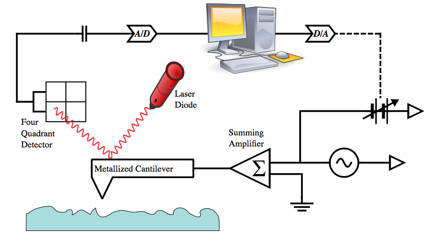
Kelvin probe force microscopy. Image by Inkwina — Own work. Licensed under CC BY-SA 4.0, via Wikimedia Commons.
Of course, Kelvin probes are not only variable in terms of their application but also in their design. For instance, the movable electrode has a few potential shapes, such as a circular plate and a narrow tip. Having a circular plate enables the probe to form a parallel plate capacitor. This type of capacitor produces a large capacitance change and current that can be measured without needing a complex electrical compensation scheme. When the probe has a narrow tip, it can scan an area and generate a lateral resolution. This option requires an electrical compensation circuit because the capacitance change and resulting current are low.
To analyze different probe geometries and their sensitivity, a research team from the Institute for Fast Mechatronic Systems at Heilbronn University and the Faculty of Electrical Engineering at the University of Applied Science used COMSOL Multiphysics simulations. Their goal was to study the capacitance characteristics of a Kelvin probe and determine optimal geometries.
Optimizing a Kelvin Probe Geometry with Simulation
The research team’s 2D axisymmetric Kelvin probe model includes both a vibrating and fixed electrode. The movable electrode (located above the fixed electrode) has a prescribed harmonic displacement and defined contact potential difference. In addition, its movement is set up as a sine wave. The fixed electrode is fixed mechanically and set to an electrical ground.
Simulation is ideal for analyzing Kelvin probes because models of analytical plate capacitors become more inaccurate as their radii are scaled down to the submillimeter domain.
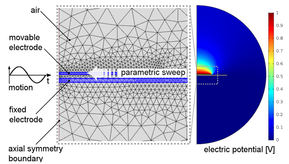
2D Kelvin probe geometry. Image by S. Ciba, A. Frey, and I. Kuehne and taken from their COMSOL Conference 2016 Munich paper.
The researchers used this model to perform parametric sweeps to test various lateral dimensions and lengths of the movable electrode. They also analyzed different tip geometries. Let’s take a look at the results…
Testing Different Probe Radii and Lengths
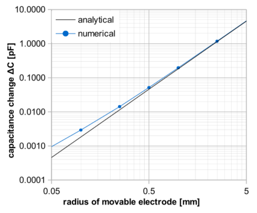
The stepwise simulations show individual effects when the probe radii and lengths are tested separately. Regarding the lateral dimensions, different movable electrode radii are studied while the length is kept constant. The simulations show that, as mentioned above, the simple analytical formula for parallel plate capacitors becomes less accurate for smaller radii, making numerical analysis indispensable.
Nominal capacitance (left) and capacitance change (right) for different radii. Images by S. Ciba, A. Frey, and I. Kuehne and taken from their COMSOL Conference 2016 Munich paper.
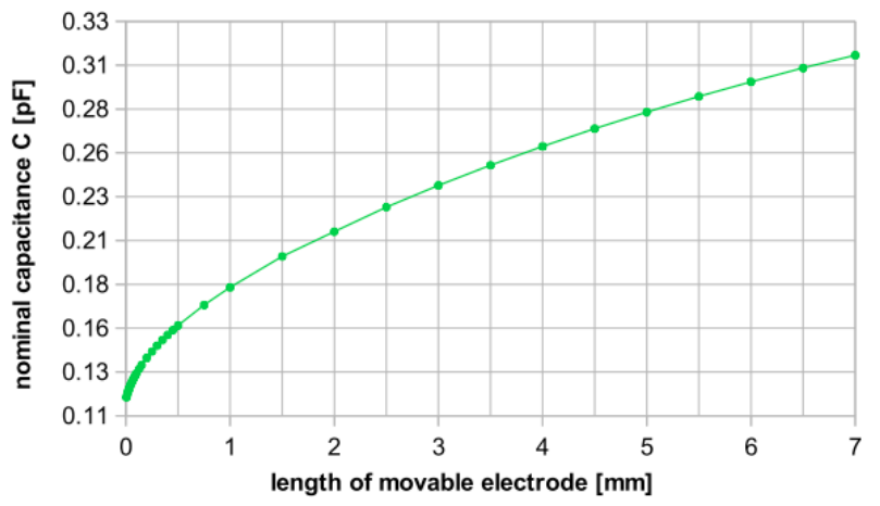
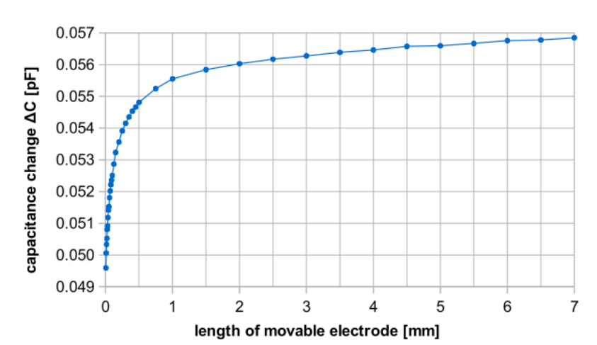
In the probe length simulations, different lengths are tested with a constant radius. These simulations show that the capacitance change and the nominal capacitance vary with the length in a different way. For a probe length less than about 2 mm, the capacitance change shows a significant decrease. This result indicates that the Kelvin probe needs to maintain a minimum length.
Nominal capacitance (left) and capacitance change (right) for different lengths. Images by S. Ciba, A. Frey, and I. Kuehne and taken from their COMSOL Conference 2016 Munich paper.
So far, we’ve only looked at the simulation results for the probe radius and length separately. However, the research shows that reducing the probe’s radius and length at the same time dramatically increases the individual effects on the probe.
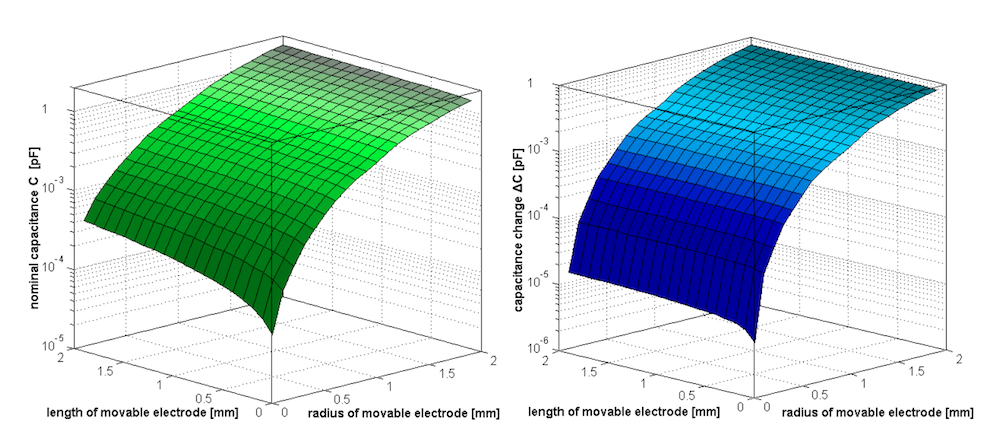
The nominal capacitance (left) and capacitance change (right) of the movable electrode as a function of the length and radius. Images by S. Ciba, A. Frey, and I. Kuehne and taken from their COMSOL Conference 2016 Munich paper.
To learn more about these geometry changes, the researchers performed additional postprocessing studies. The results reveal that each geometry must be reviewed separately due to the lack of fixed proportion between length and radius for analytical simplifications.
Comparing 3 Tip Geometries
To find the optimal tip geometry for Kelvin probes of different sizes, the researchers compared three different tip geometries:
- Flat
- Round
- Spiky
The tip geometries lead to a variety of electric energy densities, causing them to generate different capacitance behaviors.
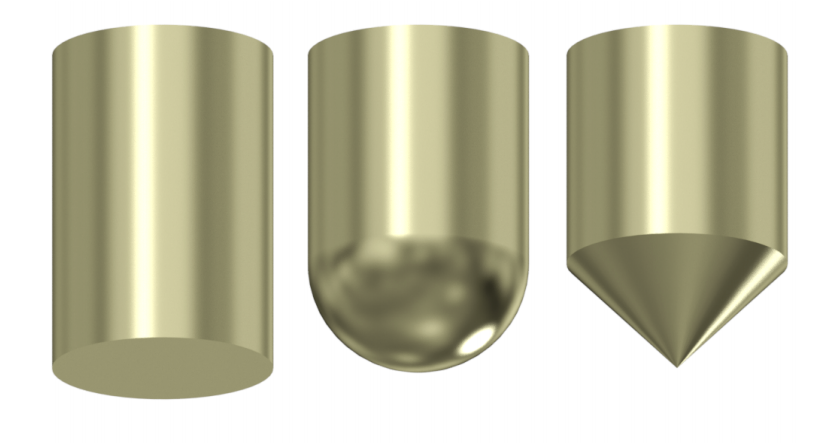
Flat (left), round (middle), and spiky (right) tip geometries. Images by S. Ciba, A. Frey, and I. Kuehne and taken from their COMSOL Conference 2016 Munich paper.
In this analysis, the length is kept constant at 2 mm and the radius is swept. To generate more precise calculations for the different geometries while still allowing for sine movement and parametric sweeps, the model includes various airspace domains for ease of meshing, such as the one shown below for the round tip.
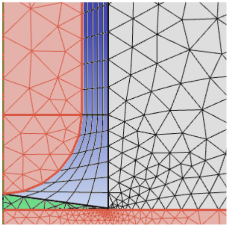
The airspace meshing for a round tip geometry. Image by S. Ciba, A. Frey, and I. Kuehne and taken from their COMSOL Conference 2016 Munich paper.
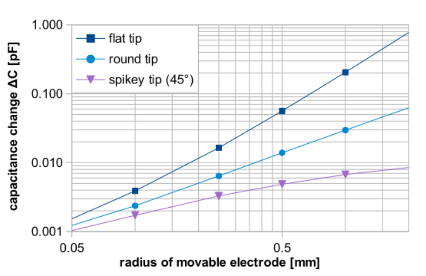
The simulations show that the flat tip design has the highest nominal capacitance and capacitance change. Additionally, the capacitance values become closer for all three geometries when the tips have smaller lateral dimensions. Note that at these small scales, using narrow tips becomes less important.
Nominal capacitance (left) and capacitance changes (right) for different tips. Images by S. Ciba, A. Frey, and I. Kuehne and taken from their COMSOL Conference 2016 Munich paper.
As shown below, the electric potential for all three geometries is comparable in the close gap. Stray capacitances are accounted for and found to only have a small influence on the Kelvin probe.

Electric potential for a flat (left), round (middle), and spiky (right) tip geometry. Images by S. Ciba, A. Frey, and I. Kuehne and taken from their COMSOL Conference 2016 Munich paper.
Finding an Equivalent Electrical Measurement Circuit
A final point of study is determining a suitable equivalent circuit. Here, a simple load resistor is added to the model to study a complete Kelvin probe setup.
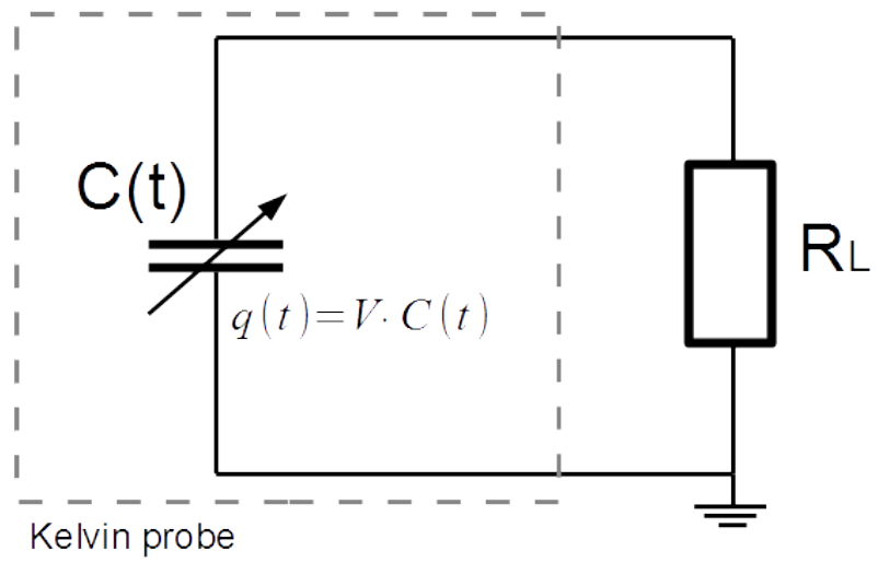
An equivalent electrical circuit of a Kelvin probe, used for a simple voltage measurement. Image by S. Ciba, A. Frey, and I. Kuehne and taken from their COMSOL Conference 2016 Munich paper.
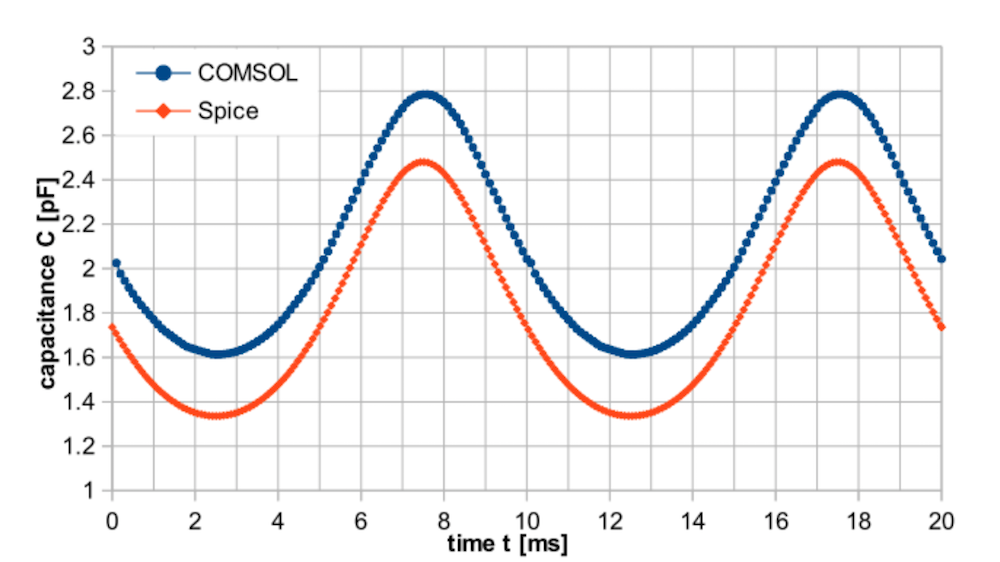
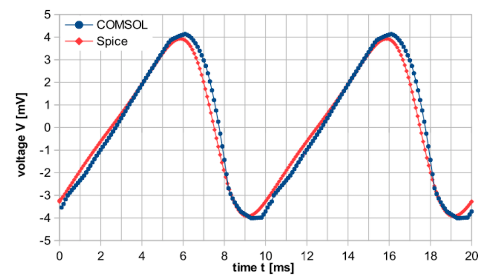
The capacitance characteristics are calculated for a Kelvin probe with an electrical circuit and a voltage drop over the load resistor. When compared to a SPICE model based on the analytical equations of a plate capacitor, these results show a good correlation.
Comparison of the COMSOL Multiphysics simulation and SPICE model for the characteristic transient capacitance behavior of a Kelvin probe with an electrical circuit (left) and for the transient voltage drop over the load resistor (right). Images by S. Ciba, A. Frey, and I. Kuehne and taken from their COMSOL Conference 2016 Munich paper.
The research team’s results offer insight into ways to optimize the geometry of a Kelvin probe. In the future, the researchers plan to design a highly sensitive electrical circuit to further optimize the probe’s performance.





Comments (0)