
Engineers use signal integrity (SI) analyses to generate information on the quality of electrical signals. They can then make design improvements based on this information. A useful technique for SI applications is time-domain reflectometry (TDR), which finds discontinuities in signal paths. Here, we use simulation to perform TDR analyses for two different designs: a high-speed interconnect and a set of parallel microstrip lines.
Signal Integrity and Time-Domain Reflectometry Analysis
As technology progresses, there is an increased demand for high-speed devices that can handle higher data rates. For these devices to perform well, they need to maintain a high signal quality. However, the quality of a signal can be distorted or degraded by a variety of factors, including:
- External noise
- Impedance mismatch
- Insertion loss
- Crosstalk
A key step in achieving a high signal quality is SI analysis. An SI analysis examines the quality of an electrical signal transmitted through an electrical circuit. With this information, engineers can locate potential SI issues and minimize them in a design. For this purpose, engineers use TDR analyses to predict the quality of a signal that is transmitted through the circuit of a device. TDR works by releasing energy into a system. The system can then be analyzed by observing the reflected energy.
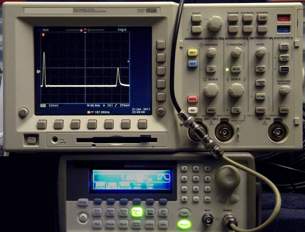
A simple time-domain reflectometer. Image in the public domain, via Wikimedia Commons.
To address issues in signal quality, we can use RF simulation to efficiently perform TDR analysis and generate results. Let’s look at two examples that are simulated in the time domain using the Electromagnetic Waves, Transient interface, available with the RF Module:
- A high-speed interconnect that deals with an impedance mismatch on a transmission line
- Adjacent microstrip lines that are impacted by an unwanted coupling or crosstalk
Example 1: High-Speed Interconnect
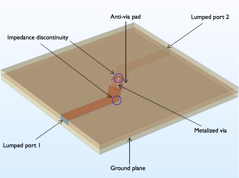
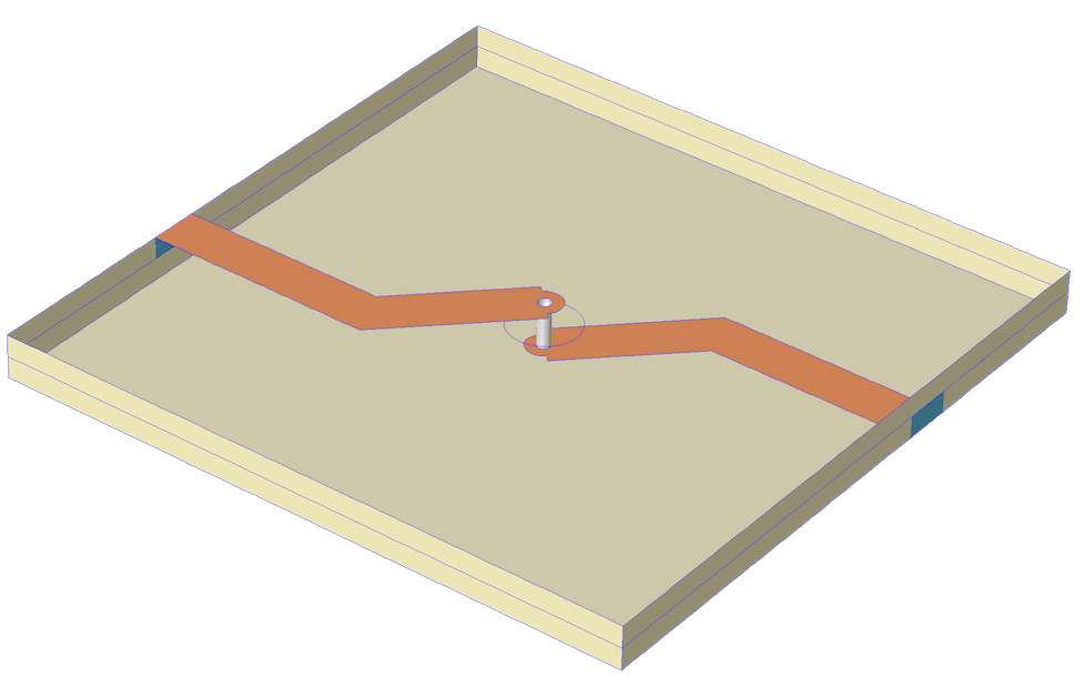
The interconnect example involves a circuit board composed of multiple dielectric layers, each of which uses a microwave substrate. Microstrip lines are located on the top and bottom of the stacked dielectric layers and are connected by a metalized via hole. There is also a ground plane with an antivia pad between the different dielectric layers.
Geometry of a high-speed interconnect.
To excite the microstrip line, this model uses a staircase step function that acts like an input signal. The function uses a fast rise time to prevent unwanted high-frequency components in the signal.
Simulation Results for the Interconnect
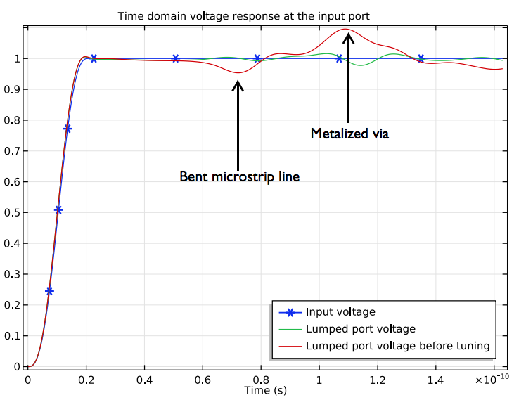
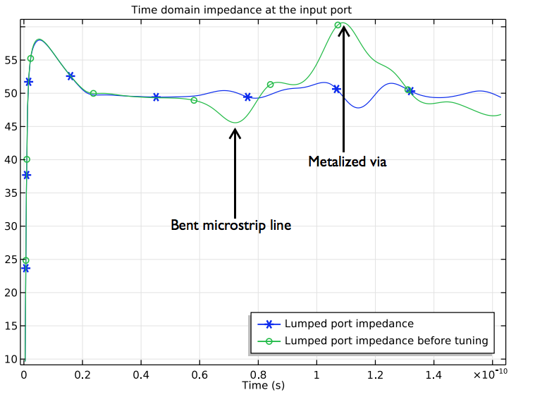
For the high-speed interconnect example, we analyze the TDR impedance and voltage at lumped port 1. By looking at the reflected signal, we can identify discontinuities in the signal path at this point. These discontinuities are seen in the plots below in the red (left) and green (right) lines. To address these issues, we tune the geometry of the microstrip line and metalized via hole, which are the two major parts with impedance mismatch. The goal with these changes is to alter the parts of the geometry that experience discontinuities, thereby reducing the signal distortion.
The time-domain voltage (left) and impedance (right) at lumped port 1 before and after tuning.
Regarding the microstrip line, the undershoot of the TDR indicates that, before tuning, the effective width at the bent part is wider than a 50-Ω line. We can fix this by using a chamfer geometry operation to trim the corner of the bent part, which results in a mitered bend. The new shape reduces the discontinuity of the bent microstrip line, helping to remove the unwanted undershoot of the TDR response.
As for the metalized via hole, the original radius size is too small, causing the via to have a high inductance. To solve this problem, we increase the radius of the via hole, which minimizes the overshoot response.
The graphs above show that these geometry changes help suppress the undesired voltage fluctuations from the discontinuities and bring the impedance closer to the ideal 50 Ω. Thus, by identifying signal path discontinuities, a TDR simulation analysis can help us improve a high-speed interconnect design.
Example 2: Parallel Microstrip Lines
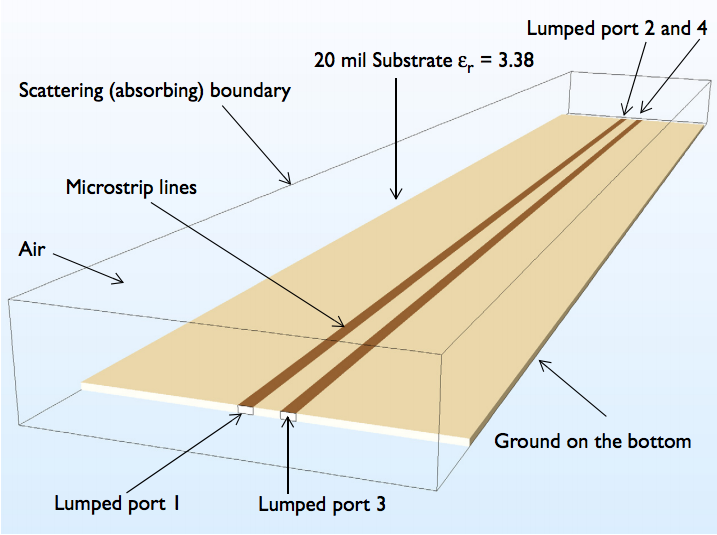
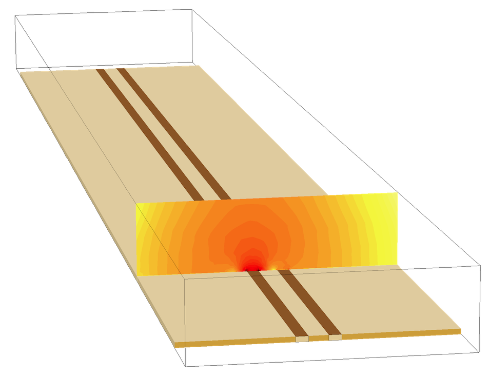
In our second example, we focus on how crosstalk affects two parallel microstrip lines. The lines are located on a microwave substrate that has a consistent dielectric constant.
Geometry of a microwave substrate with parallel microstrip lines.
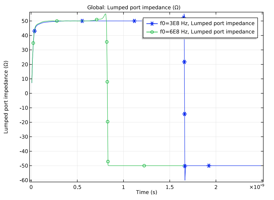
In this simulation, we apply two pulses and set their widths to half of the 300-MHz and 600-MHz signals. The pulse widths now correspond to data rates of 600 Mbit/s and 1.2 Gbit/s, respectively. During the simulation, we can switch the frequency of the pulse by applying a parametric sweep.
Simulation Results for the Microstrip Lines
For the example of the adjacent microstrip lines, we start by looking at the excitation port (lumped port 1). In the left graph below, we see the TDR of the port with respect to impedance. The signal level is 1 V and the calculated port impedance is around 50 Ω. On the right, we examine the voltage and input pulse signal at this port. There is no distortion in the port voltage because the input signal moves through a straight 50-Ω line and terminates with a 50-Ω resistor without any discontinuity in the line.
The impedance (left) as well as the input pulse and voltage (right) at lumped port 1 for data rates of 600 Mbit/s and 1.2 Gbit/s.
At the corresponding through port (lumped port 2), we see a discontinuity. Here, the TDR response of the 1.2-Gbit/s signal is slightly distorted when it reaches 1 V. On the other hand, the lower MHz case (the signal at 600 Mbit/s) appears undistorted.
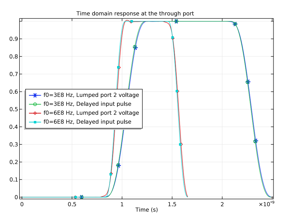
The delayed input pulse and voltage at lumped port 2 for data rates of 600 Mbit/s and 1.2 Gbit/s.
Moving on, let’s investigate a key metric for this study: the crosstalk between the microstrip lines. We start with lumped port 3, which is located near the excitation point. Here, the coupled signal level between the two data rates is similar. At lumped port 4, which is near the through port, the higher data rate signal generates a stronger crosstalk on another signal path.
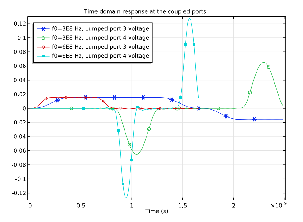
The voltage at lumped ports 3 and 4 for data rates of 600 Mbit/s and 1.2 Gbit/s.
These results show that signals at higher frequencies and data rates result in increased distortion and stronger crosstalk. With this information, we can design high-speed devices that effectively handle high data rates.
Learn More About Electromagnetics Simulation in COMSOL Multiphysics®
- Download the tutorial models highlighted in this blog post:
- Read a related blog post on designing microwave circuits:




Comments (0)