Since 1901, the Royal Swedish Academy of Sciences has recognized significant contributions to the field of physics with a Nobel Prize award. This year’s Nobel Prize in physics was presented to a team of scientists from Japan and the U.S., recognizing their work in developing blue light emitting diodes (LEDs). Let’s take a closer look at the innovative research behind this lighting technology.
Meet the Winners of the 2014 Nobel Prize in Physics
This year’s winners — Isamu Akasaki from Maijo University in Nagoya, Japan; Hiroshi Amano from Nagoya University in Japan; and Shuki Nakamura from the University of California, Santa Barbara — have joined a list of 196 other notable physics laureates who have received the Nobel Prize in physics. In the early 1990s, these researchers successfully developed the first blue LEDs, a technology that had long posed a challenge to researchers and industries.
The primary obstacle was finding the right material to use. An LED is composed of layered semiconductor materials in which electrons move to create illumination. The energy band gap of the semiconductor determines the color of the light that is emitted. While gallium arsenide was used in the production of red and green LEDs, this material proved inefficient in creating blue light.
Why? Blue light requires an extremely high energy gap in order to be produced.

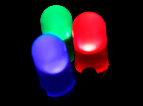
The color of an LED light depends on the semiconductor’s energy band gap. (“RGB-LED” by PiccoloNamek. Licensed under Creative Commons Attribution-Share Alike 3.0 via Wikimedia Commons).
The scientists found a solution to this issue in a wide bandgap semiconductor material known as gallium nitride. In 1986, Akasaki and Amano successfully grew large crystals of the compound on a scaffold designed with a layer of aluminum nitride on a sapphire substrate. In the development of his blue LED, Nakamura manipulated temperature to foster growth of the crystals, with the first layer of gallium nitride grown at a low temperature and additional layers at high temperatures.
In LED devices, an active layer is located between an n-layer, a layer with excessive electrons, and a p-layer, a layer with a shortage of electrons. When a current is applied, the charge electrons come together in the active layer, producing blue light. In their research, Akasaki and Amano stumbled upon the fact that the quality of the p-layer improved when electron microscopes were used to take pictures of the material. The electrons, it turns out, were able to remove the hydrogen from the p-layer that was causing blockage. Nakamura built upon this initial finding, recognizing that heating the material enhanced the quality of the p-layer, resulting in a brighter, more efficient blue LED.
Blue LEDs: An Invention with Extensive Use
With the advent of blue LEDs came the potential for greater efficiency in lighting.
The combination of red, green, and blue LEDs allowed for the production of white LED lamps, which are used to light a number of homes and offices as well as our television, computer, and cell phone screens. These lamps offer an advantage over traditional incandescent light bulbs in which light is created by the heating of a wire filament with an electric current passing through it. In addition to having a longer life span, LED lamps waste less heat and require lower voltage to power than incandescent bulbs, helping to reduce electricity costs and decrease greenhouse gas emissions.
Because of the low level of energy needed to operate LED lights, this technology also offers potential in helping individuals who live in areas outside of an electricity grid. The efficiency of LEDs could make them a resource in the developing world, generating solar-powered energy for homes and buildings.

A blue LED signals the end of a train platform. (“Shenzhen Metro blue LED warning light between trains and platform” by Zhengruiw02 — Own work. Licensed under Creative Commons Attribution-Share Alike 3.0 via Wikimedia Commons).
Analyzing Thermal Management in LED Lighting
An important area of research in LED lighting is thermal management. Heat sinks are often used in LED lamps as a means to draw heat from the light itself and dissipate it into the air.
In a previous blog post, we highlighted the work of Veryst Engineering in simulating LED lighting designs and thermal stresses that result from their complex geometries and high temperatures. Using COMSOL Multiphysics and the Particle Tracing Module, the team was able to show the temperature in and around the bulb. While the heat sink helped to dissipate some of the heat, the low flow velocities in the vicinity around the light bulb suggested that further measures could be taken to optimize the design. Modeling and simulation was used to increase the flow velocities around the bulb, utilizing natural convection in driving heat away from the actual light.
A research team from the University of Houston in Texas also investigated the use of thermal management in LED lighting systems. As noted in the study, heat sink LED lighting applications require materials that are thermally conducting but electrically insulating. To meet this need, the team altered polymers by mixing them with metal nanoparticles. This compound allowed for the particle’s surface to be changed while still holding on to its bulk properties. Their results indicated that these core-engineered shells effectively managed heat within the light source while enhancing the dieletric properties of the polymer.


Comments (0)