
Compliance testing is used to ensure that various products, processes, and systems meet standard requirements. Just as important as these tests is the equipment used to perform them. This testing equipment must be designed so that it delivers precise measurements that are reflective of real-world performance. RF modeling is a useful approach to analyzing and optimizing such devices, generating greater confidence in the measurements they obtain. To showcase this, we’ll look at a well-known equipment choice in EMC/EMI testing…
Equipment Required in EMC/EMI Testing
Does an electronic or electrical device operate as it should in a common electromagnetic environment? Before such a product is of the quality and safety to bring to market, this is an important question to address. This question is at the heart of EMC/EMI testing, and finding the answer helps us modify operations as needed.
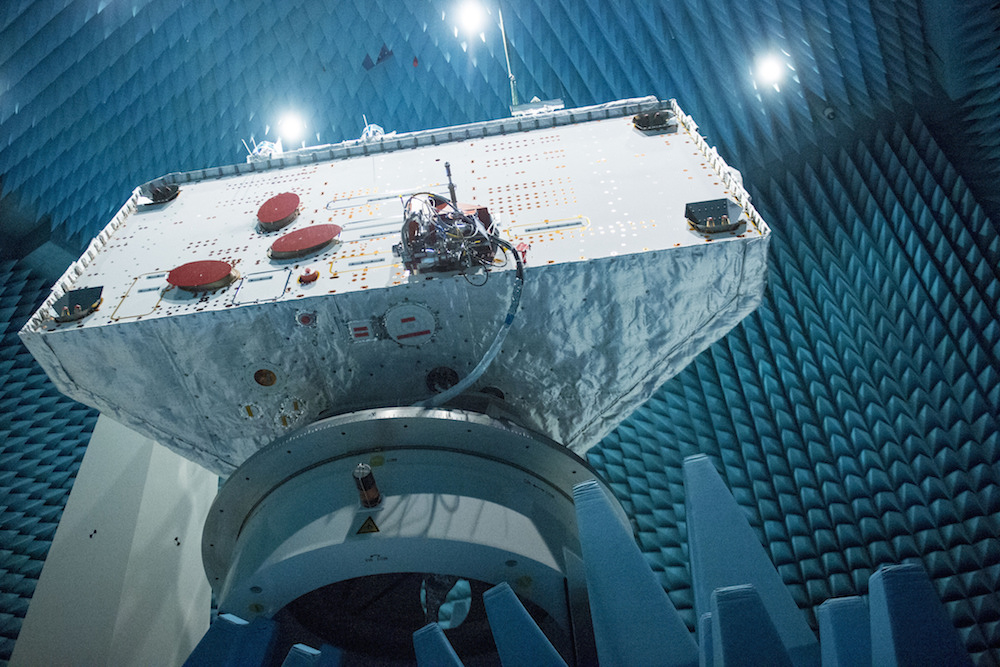
A spacecraft undergoes EMC/EMI testing. Image by ESA-G Porter. Licensed under CC BY-SA 3.0 IGO, via Flickr Creative Commons.
When thinking about EMC/EMI testing, we can divide its focus into two classes: emissions and susceptibility. On the emissions front, tests point out unwanted emissions and potential countermeasures that could reduce the electromagnetic energy that is generated. In the case of susceptibility, testing shows how devices react in the presence of radio frequency waves, where there is a tendency for breakdown to occur. By achieving immunity, devices can function as normal when encountering unwanted emissions.
Running EMC/EMI tests requires specific equipment. Log-periodic antennas are one of three well-known test antennas used for this purpose. (We discussed one of the other well-known types, a biconical antenna, a little while back.) The coplanar dipole array type — a popular form of this wideband antenna — is often placed inside an anechoic or reverberation chamber and used to obtain antenna measurements in the UHF range.
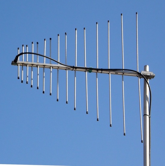
An example of a log-periodic antenna. Image by K. Krallis, via Wikimedia Commons.
Before these antennas are ready to obtain EMC/EMI measurements, it is important that their designs are analyzed to ensure accuracy. The COMSOL Multiphysics® software and the RF Module can be used to optimize these designs.
Using RF Modeling to Analyze the Design of a Log-Periodic Antenna
When looking at a log-periodic antenna, you may notice that its shape is similar to a Yagi-Uda type of antenna. However, the way these two antennas work is quite different. A log-periodic antenna achieves a wider frequency response (bandwidth) through a coplanar array, while a Yagi-Uda antenna achieves a higher gain (directionality) through a driven element and multiple passive elements.
To help our log-periodic antenna take shape, we fit a coplanar diode array through a few metallic body frames. These frames and the metallic dipole rods are modeled with perfect electric conductor (PEC) boundary conditions, as surface loss is negligible for the relative frequency range. Note that the interior portion of the antenna’s body is excluded from the modeling domain, including frames and rods where wave propagation is not anticipated.
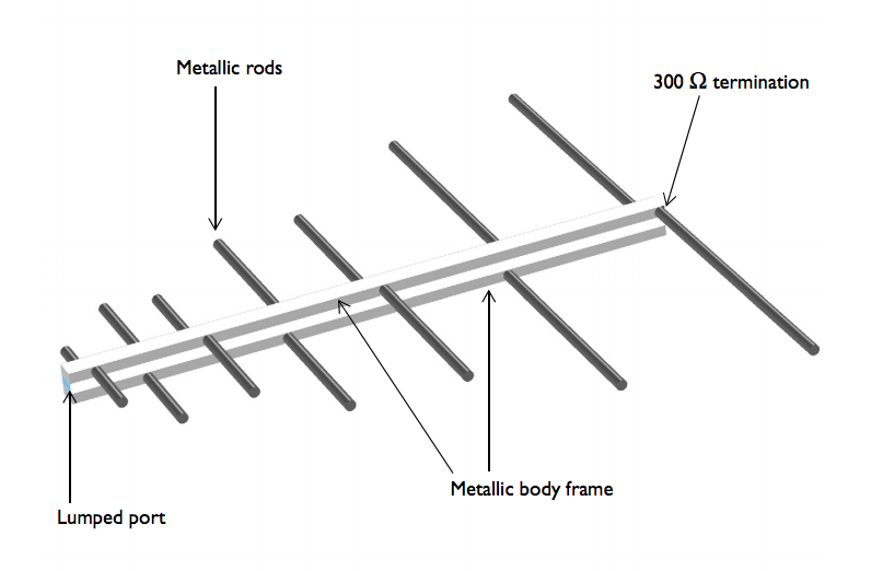
The configuration of the log-periodic antenna.
The antenna is excited via a lumped port that is placed between two body frames at the end of one gap, where a shorter pair of rods is located. To terminate the electric field, a 300-Ω resistor is added to the other end of the gap, where a longer pair of rods is located. The model itself is housed in a spherical domain enclosed by perfectly matched layers (PMLs) that absorb any outgoing radiation.
Note that the length of the dipole rods decreases gradually with a ratio that is constant to the lumped port. Further, with parameterized geometry parts, it is easy to build the repeated pattern for the radiating structure.
To visualize the impedance matching properties, a Smith plot is generated, with the different colors representing different frequencies. The frequency-swept impedance normalized by 50 Ω is plotted near the point shifted from the middle of the plot (approximately 68 Ω).
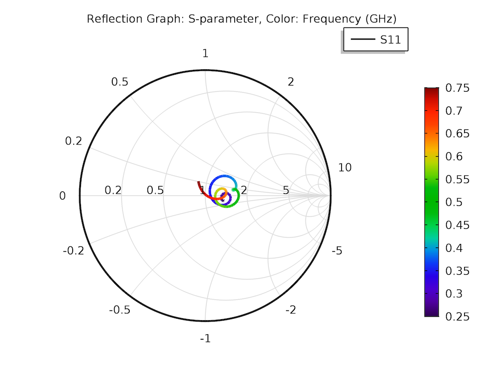
Smith plot displaying the impedance matching properties.
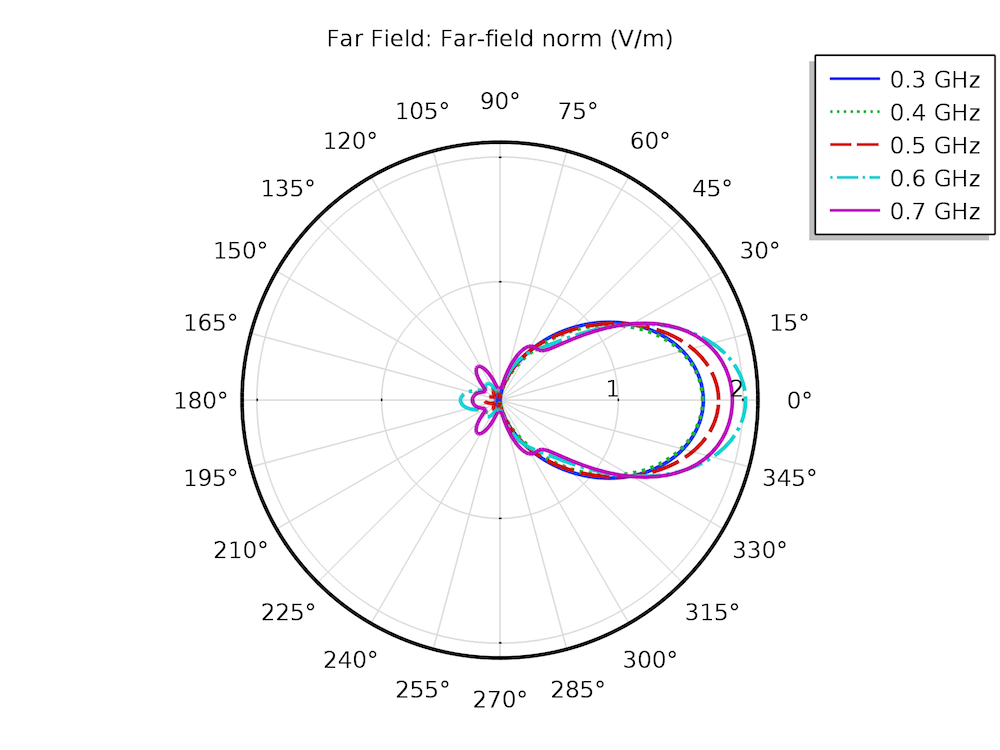
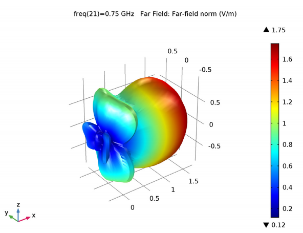
The next set of plots depicts the far-field radiation pattern. In the 2D polar plot, with the radiation directed toward the lumped port, we can see a slight variation in the pattern’s directionality as the frequency increases. This tendency is also reflected in the 3D simulation plot. Note that in the case of the 3D plot, a finer angular resolution could be applied to accurately visualize the sidelobes.
The far-field radiation pattern depicted in a 2D polar plot (left) and 3D simulation plot (right).
Lastly, we consider the computed voltage standing wave ratio (VSWR). The results show that the impedance of the antenna is near 50 Ω for the simulated frequencies — a ratio that is better than 2 to 1. Such wideband impedance matching properties are important for the accuracy of measurements obtained in EMC/EMI testing.
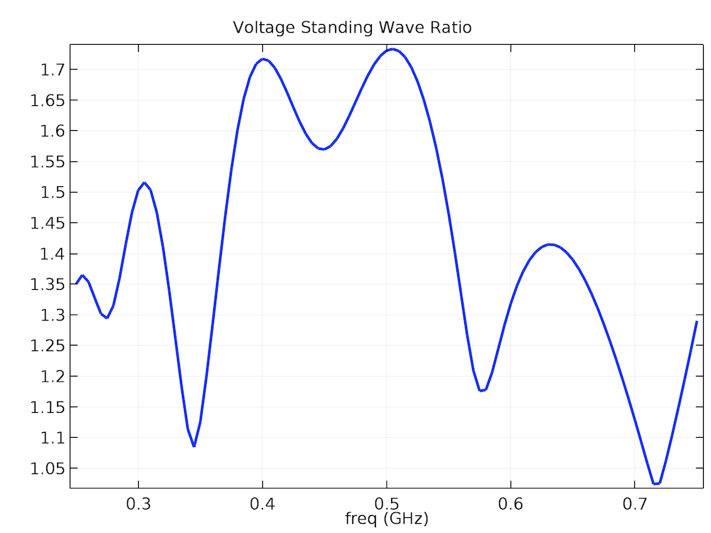
The antenna’s computed VSWR.
Ready to give this tutorial model a try? Simply click the button below…
Note that you can also access this tutorial from the Application Library in the COMSOL Multiphysics software.
Further Resources
Here are more tutorial models that focus on simulating the EMI/EMC testing environment:




Comments (0)