
Infrared (IR) light has applications in various fields, including thermal imaging, night vision, biomedical sensors, and more. Due to the high refractive index of the materials used to make the lens and window of IR cameras, a significant fraction of light gets reflected back (~30% in silicon and ~21% in cadmium zinc telluride). The conventional approach to overcome such challenges is to use multiple layers of dielectric coatings, but this poses challenges such as limited bandwidth; narrow acceptance angle; and loss of adhesion between the thin layers while operating at high temperatures (for example, lasers). One way to overcome such challenges is to etch the top surface of the lens or window with a particular pattern in order to enhance the transmittance within the infrared spectrum. However, analyzing the transmittance of different etched patterns on the lens and windows requires multiple design iterations before finalizing the product.
Editor’s note: This blog post was updated on November 9, 2021, to include a discussion of the broadband optimization of a microstructure.
Simulating Different Design Patterns for Antireflecting Microstructures
Simulation is one the smartest ways to tackle the issue of high fabrication expenses. You can simulate different patterns and their intricacies to enhance the transmittance of the final prototype, which can then be given for fabrication. In this blog post, we explore how two microstructure designs can improve the bulk transmittance of silicon (~70%) and cadmium zinc telluride (~79%) to more than 90% within the specific wavelength spectrum. The two microstructure designs are:
- Rectangular
- Pyramidal
As shown in the image below, the bulk silicon can be etched at the top with an array of rectangular microstructures. However, instead of modeling the array of rectangular microstructures over the bulk silicon, a single unit cell along with a periodic condition can be simulated. This approach significantly reduces the computation time of the model without impeding the accuracy of the results. You can certainly analyze a 3D unit cell in the COMSOL Multiphysics® software, however, in order to keep the analysis simple, and still gain a lot of insight, we will instead showcase an approach to model a simple 2D cross section of a 3D unit cell model.
![]()
The bulk silicon can be replaced with an array of rectangular microstructures on bulk silicon. The unit cell model with periodic conditions replicates the array of rectangular microstructures on bulk silicon.
Rectangular Microstructure with Silicon Substrate
The bulk transmittance of silicon is estimated to be about 70%. The other 30% is reflected and lost in the environment. In this section, we will discuss how the array of rectangular microstructures etched on the top of a Si substrate can enhance the transmittance by more than 90% while operating in the infrared spectrum between 2.6 μm and 4.5 μm. The transmittance of the bulk Si etched with rectangular microstructures for different angles of incidence (0–80°) is also analyzed.
The rectangular etch pattern is performed on the complete silicon bulk substrate. However, for simplicity, we consider a 2D cross section unit cell model, as shown in the figure below. The height and width of the rectangular pattern along with the pitch of the unit cell can be varied to change the transmittance profile within 2.6 μm and 4.5 μm.
In this model, the pitch of the unit cell is considered to be 780 nm, while the height and width of the rectangle is considered to be 450 nm and 125 nm, respectively. The Floquet periodic condition can be applied on either side of the unit cell. The Port condition, with the type of port set as Periodic, can be selected to launch the electromagnetic plane wave polarized in the z direction (out of plane) and propagating in the -y direction (downward). Out-of-plane (m =±1) diffraction orders are added in Port 2 in order to account for higher-order diffraction.
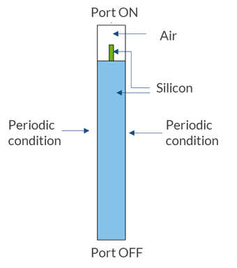
Boundary conditions for setting up a unit cell of a rectangular microstructure.
First, a wavelength domain study is performed while sweeping from 2.6 μm to 4.5 μm with a step of 0.1 μm. Then, a wavelength domain study with the operating wavelength as 3 μm is performed while sweeping the angle of incidence (mentioned in the Port boundary condition) between 0 and 80° with a step of 1°. It can be observed that the transmittance from the bulk silicon (~69%) can be improved to more than 92% within 2.6 μm and 4.5 μm with normal incidence. In the incidence angle sweep study, the transmittance significantly declines after 40°.
![]()
0th-order transmittance of the silicon rectangular microstructure with a varying operating wavelength.
![]()
0th-order transmittance of the silicon rectangular microstructure while operating at 3 μm with respect to angles of incidence.
Pyramidal Microstructure with Cadmium Zinc Telluride Substrate
The bulk transmittance of cadmium zinc telluride (CZT) is estimated to be about 79%. The other 21% is reflected and lost in the environment. In this section, we will discuss how the pyramidal microstructure etched on top of a CZT substrate can enhance the transmittance to be more than 90% while operating in the infrared spectrum between 7 μm and 14 μm. The transmittance of the bulk CZT etched with a pyramidal microstructure for different incidence angles (0–80°) is also analyzed.
In this model, the pitch of the unit cell is considered to be 2.4 μm, while the height of the pyramid is considered to be 5 μm. The width of the top edge of the pyramid is considered to be 100 nm. Again, the Floquet periodic condition is applied on either side of the unit cell, while the Port condition, Periodic type, is chosen to launch the electromagnetic plane wave polarized in the z direction (out of plane) and propagating in the -y direction (downward). Out-of-plane (m =±1) diffraction orders are added in Port 2 in order to account for higher-order diffraction.
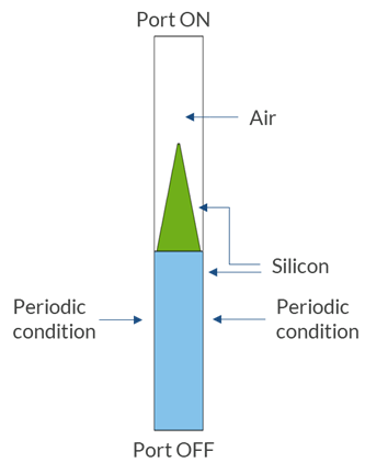
Boundary conditions for setting up a unit cell of a pyramidal microstructure.
First, the wavelength domain study is performed while sweeping from 7 μm to 14 μm with a step of 0.2 μm. Then, the wavelength domain study with operating wavelength as 7.5 μm is performed while sweeping the angle of incidence (mentioned in the Port boundary condition) between 0 and 80° with a step of 1°. It can be observed that the transmittance from the bulk silicon (~79%) can be improved to more than 94% within 7 μm and 14 μm with normal incidence. In the incidence angle sweep study, the transmittance significantly declines after 27°.
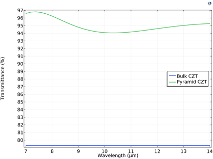
0th-order transmittance of the CZT pyramidal microstructure with varying operating wavelengths.
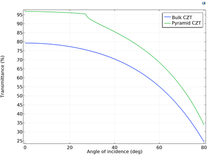
0th-order transmittance of the CZT pyramidal microstructure while operating at 7.5 μm with respect to angles of incidence.
Broadband Optimization of a Microstructure
Moreover, the question can be posed of whether the broadband transmittance of the rectangular and pyramidal geometry can be further improved. To answer this question, a gradient-free broadband optimization is set up for the rectangular and pyramidal microstructure by defining the following objective function:
^2 \]
where \lambda_{min} and \lambda_{max} are the minimum and maximum operating wavelength respectively, T_e = 100*realdot(ewfd.S21,ewfd.21) = 100*|ewfd.S21|2, and T_t = 100. The objective function tries to optimize the transmittance in the whole spectrum to be close to the target transmittance of 100 %.
For the rectangular microstrucure, the above objective function is set up with two control parameters: w_{pillar} (pillar width) and h_{pillar} (pillar height), which are subject to the constraints:
For the pyramidal microstructure, the same objective function is set up with three control parameters: wb_{pyramid} (pyramid bottom width), wt_{pyramid} (pyramid top width), and h_{pyramid} (pyramid height), which are subject to the constraints:
The subscripts L and U represent the lower and upper bounds of the constraint.
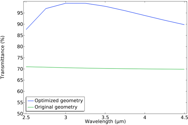
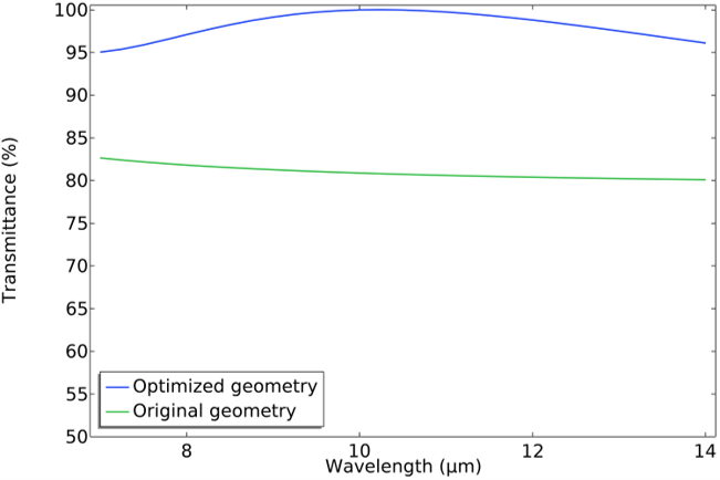
The complete details of the broadband optimization is described in the tutorial model. The optimization study was set up to minimize the objective function by varying the control parameters within the ranges from the lower bounds to the upper bounds. For the rectangular microstructure, the broadband optimization was performed between 2.5 μm and 4.5 μm, while for the pyramidal microstructure, the broadband optimization was performed between 7 μm and 14 μm.
The results of the gradient-free broadband optimization for the original and optimized geometries are shown in the figures and summarized in the tables below.
Comparison of the transmittance of the original and optimized geometry for a rectangular (left) and pyramidal (right) microstructure.
The following table summarizes the geometry parameters for the rectangular microstructure:
| Parameters | Original Geometry | Optimized Geometry |
|---|---|---|
| Thickness of the pillar | 50 nm | 111.32 nm |
| Height of the pillar | 100 nm | 461.67 nm |
The following table summarizes the geometry parameters for the pyramidal microstructure:
| Parameters | Original Geometry | Optimized Geometry |
|---|---|---|
| Top width of the pyramid | 50 nm | 50 nm |
| Bottom width of the pyramid | 0.5 μm | 0.9 μm |
| Height of the pyramid | 0.5 μm | 2.25 μm |
Concluding Thoughts
Using simulation, we are able to determine that the rectangular silicon microstructure could increase the transmittance of bulk silicon (~70%) to more than 90% between the 2.6 μm and 4.5 μm spectrum, while the pyramidal CZT microstructure could increase the transmittance from bulk CZT (~79%) to more than 94% between the 7 μm and 14 μm spectrum. We can also observe that the transmittance decreases when the angle of incidence increases for both the rectangular silicon and pyramidal CZT microstructures. The broadband transmittance of these microstructures can be further enhanced by performing gradient-free broadband optimization, as discussed in this blog post.
Next Step
Want to try modeling microstructured antireflective coatings for infrared wavelengths? Click the button below to access the MPH files for the models discussed here.
You can also try these related tutorial models:
- Antireflective Coating with Multiple Layers
- Broadband Optimization of Microstructured Antireflecting Coating
Reference
- D.S. Hobbs, B.D. MacLeod, “Design, fabrication, and measured performance of anti-reflecting surface textures in infrared transmitting materials,” Proc. SPIE 5786, Window and Dome Technologies and Materials IX, pp. 349–364, 2005.




Comments (3)
Ivar KJELBERG
July 8, 2021Nice Blog,
Now, to go one step further, one may put such structures on a MEMS deforming structure, within a waveguide cavity and get tunable filters …
Have never had time to push this idea, it was proposed by a colleague some 25 years ago for our MEMS designers, but we did not have the tools at that time to optimise and see the true benefit of such structures, hence to sell efficiently the idea internally.
Now its possible, but my time is “over” so it’s for you out there, the next “generation” 🙂
Have fun COMSOLing,
Sincerely Ivar
Uttam Pal
July 8, 2021 COMSOL EmployeeHi Ivar,
It’s an excellent piece of advice. We have taken note of it and would definitely see if we can move towards tunable filters, which would be a multiphysics problem. Thanks again.
Collins Kariuki
March 14, 2024Where can I get the .mph files? They are no longer there. There’s only a powerpoint presentation. I would like access to the .mph files since I am interested in learning how you plotted angle of incidence on the x-axis. Right now, I only know how to put wavelength on the x-axis.