What’s a penny made of? Though they appear to be solid copper coins, they actually don’t contain much copper at all these days. Instead, the U.S. Mint saves money by applying only a veneer of valuable metal onto a less expensive one. Have you ever thought about the manufacturing process by which this is achieved? Let’s find out.
Electroplating
A U.S. penny is made of zinc with a 20 microns thick layer of copper on its surface. When we make the coin, its manufacturing process must be controlled. If pennies were produced in different weights, sizes, or colors, people would have no confidence in the currency. The greater the natural variation in a currency as minted, the easier it is to forge. Compared to people, the demand for quality control is even higher for vending machines and coin counters, as both rely on the weight and shape of coins to function properly.
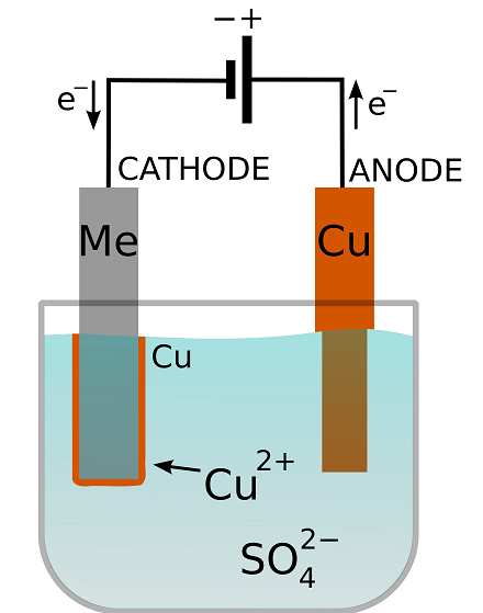
Electroplating is a common manufacturing method that involves applying a thin layer of metal onto another. This takes advantage of the fact that we are plating a metal object that conducts electricity. The object being plated is referred to as the substrate.

Schematic of an electroplating cell with a copper sulfate plating bath. The metal substrate is denoted “Me”. The transfer of electrons in the circuit is balanced by the transfer of ions in the solution. Image in the public domain, via Wikimedia Commons.
To understand how this works, let’s first think about a simple chemical reaction.
In school, you may have come across an experiment in which iron was placed into a copper salt solution. While in the solution, the metal iron spontaneously dissolved in the form of positively charged ferrous (iron) ions, leaving electrons behind. Meanwhile, the positively charged cupric (copper) ions acquired those electrons and deposited them as solid copper. On any metal surface, there is a constant chemical reaction of metal to ions in solution and ions to solid metal.
We can write this as a balanced chemical reaction:
Cu2+(aq) + Fe(s) → Cu(s) + Fe2+(aq)
where (aq) denotes a species dissolved in water and (s) represents a solid material. The superscript “2+” stands for the charge on a species.
When electroplating, a power source is used to apply a voltage to the substrate with respect to a positive electrode, called the anode. This is done to manipulate the equilibrium of this reaction. If the substrate becomes negative polarized, a cathode, the reaction of ions to metal will be favored. In other words, the voltage drives a reaction in which ions gain electrons to become solid metal. Because the electrons have to come from the conducting substrate and can’t just jump a long way into the solution, the copper is deposited on the cathode surface.
We can write this as:
Cu2+(aq) + 2e-(m) → Cu(s)
where the two electrons come from the metal.
The amount of metal deposited is proportional to the electric current passed. This is because for every atom of metal deposited, a precise number of electrons are drawn to the cathode to balance the ionic charge. In this case, we know that this number is two for cupric ions. Therefore, by measuring the passed current, we can stop the deposition when a certain amount of plating has taken place, i.e., when a certain mass of solid copper has been deposited.
Current Distribution
We still don’t know exactly where that plating occurs, however. The electrons distribute themselves throughout the conductor, so it’s impossible to tell from the measured current whether the plating is uniform or if it only occurred in one part of the substrate.
In this case, we can turn to physical modeling to predict the current distribution of copper on the surface. My colleague, Melanie, recently blogged about the different theoretical types of current distribution.
For example, we find that because sharp edges and corners of solid objects are more exposed to the plating bath, the deposition rate will be greater here (you can see this effect in the Copper Deposition in a Trench model, which is available in our Model Gallery). Ions have to travel further or in competition with other ions between the anode and more “obscure” or distant sites on the substrate. This raises the resistance of the solution along these paths and lowers the driving force for deposition.
Controlling Surface Deposition
A number of options are available for controlling surface deposition. To see illustrations on how to model these, take a look at some models made with the Electrodeposition Module.
In superfilling, a catalyst is carefully localized to selectively accelerate the reaction rate in concave regions, balancing out the current distribution over the whole object.
An alternate method is to add chemical species at the cathode surface and through different mechanisms to inhibit deposition, i.e., contrary to the catalysts and force the current density to become more uniform.
Another route is to use forced flow in the plating bath in order to specifically direct the plating solution to certain regions. In COMSOL Multiphysics, it’s convenient to be able to solve for fluid flow and surface electrochemistry together. The Fountain Flow Effects on Electrodeposition on a Rotating Wafer model provides a good example of this.
So… How Do We Make a Penny?
Of course, the U.S. Mint isn’t going to tell us how they do it or we’d all be manufacturing money at home. The techniques involved are actually quite expensive. It costs more than a penny to make a penny, which is the price the U.S. government pays for a secure currency to be handled by its citizens. A lot of this cost is due to the rising price of raw metal; whereas the U.S. Mint uses zinc for the bulk of the penny, Canadian and British pennies are made of mild steel. Both methods keep their relative face values and production costs well above their value in raw metal. This proves that the more we know about electroplating, the wider our alternative options can be!
Setting Up an Electrodeposition Model
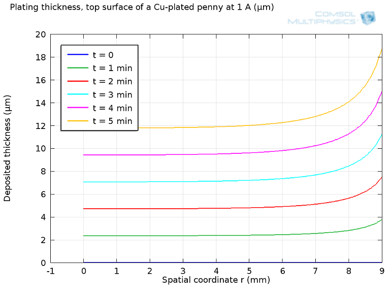
I set up a simple electrodeposition model in COMSOL Multiphysics to look at current flow to a disc-shaped substrate. I found that it’s not easy to get a uniform plating. My cell draws 1 A for five minutes, which is good enough to plate more than 20 microns thickness of copper over the surface of the substrate. However, without any particular attention, we get much more plating at the edges:

Plot of deposition thickness vs. radial coordinate for electroplating of a disk.
After five minutes, the plated penny would come out about 16 microns thicker at the edge than in the center. This is only 1% of the total thickness, which would be hard to tell for a non-specialist, but certainly noticeable to a machine or even a forger. One can only imagine how difficult it would be if the substrate to be plated has a complex pattern, such as tiny letters or Abraham Lincoln’s face, for that matter.
So, as it turns out, my first batch of pennies didn’t make the grade. Do you think you can you do better?
Governments around the world will always look for ways to save money. Many companies turn to modeling to better understand the required manufacturing process. One option they could choose is to use the Electrodeposition Module to predict the quality and expense of an operation for an electroplating cell.


Comments (0)