Schottky diodes are one of the oldest semiconductor components, but they are still found in many modern applications, including computers and radar systems. To ensure that a Schottky diode performs well, it’s important for engineers to accurately analyze factors like current density and barrier height in the design. As a benchmark model demonstrates, the COMSOL Multiphysics® software and add-on Semiconductor Module are well suited for this type of analysis.
A Brief History of the Schottky Diode
The basic principles of the Schottky diode were demonstrated in 1874 by Karl Ferdinand Braun. By joining a metal wire and galena crystal (which acted as the semiconductor), Braun created a point-contact diode that could convert alternating current into direct current (i.e., rectify the current). While this is one of the first examples of a semiconductor diode, Braun’s work didn’t gain much attention, as there weren’t any practical applications at the time.
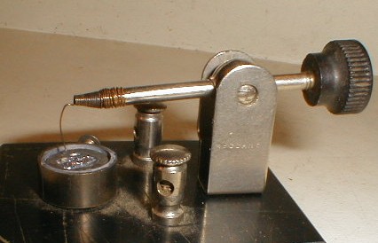
The invention of the radio led to demand for semiconductor diodes (called crystal detectors at the time). In 1901, Jagadish Chandra Bose, an Indian professor of physics, demonstrated that the diode could pick up radio waves. 5 years later, G.W. Pickard patented the “cat’s whisker detector”, a common radio component until the 1920s. This diode consisted of a thin metal wire (the so-called cat whisker) that lightly rested on a silicon crystal. By adjusting the position of the wire, you could pick up a signal, thereby tuning the radio.

A cat’s whisker detector that was once used in a crystal radio receiver. Image by JA.Davidson, via Wikimedia Commons.
In the 1930s, physicist Walter Schottky discovered that when a metal and semiconductor touch, a barrier is created between them. His work formed the basis (and the name) for Schottky diodes — also known as Schottky barriers, hot-carrier diodes, and hot electron diodes. As with other types of diodes, when a voltage is applied, the barrier generated by the contact allows current to flow in one direction (the forward bias) and stop in the other (the reverse bias).
Applications and Advantages of Schottky Diodes
Compared to other modern diodes, Schottky diodes have many benefits. For instance, Schottky diodes have a high current density and a low forward voltage drop, which means they consume less energy and generate less heat. As a result, they’re much more efficient and compact than their counterparts, and they can be built with smaller heat sinks. Other advantages include fast switching speed, short recovery time, and low capacitance — helpful qualities for applications like:
- Charging computers and smartphones
- RF mixing in radar systems
- Rectifying power for motor drives and LED lights
- Preventing transistor saturation
- Protecting against battery discharge in solar cells
To ensure that Schottky diodes perform well in these and other applications, engineers can use semiconductor simulation software to evaluate key design factors like current density and voltage. Keep reading for a look at a benchmark example.
Analyzing a Schottky Diode Design
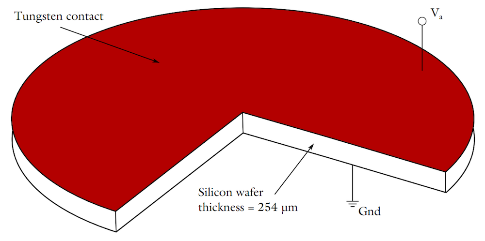
The Schottky Contact benchmark model describes the behavior of a simple Schottky diode under a forward bias. The geometry for this diode is wafer-shaped, with the semiconductor (silicon) on the bottom and the metal (tungsten) deposited on top. Note that you can easily define the properties of the silicon using the default settings in the COMSOL® software.

The geometry of a simple Schottky diode.
An important aspect to examine in a design is the height of the barrier created by the Schottky contact, as this affects whether or not the diode will work. Determining the barrier height can be a complex task, as it is based on the structure of the metal-semiconductor interface. In this model, only the ideal height is computed based on silicon’s default material properties and tungsten’s work function (4.72 V), which gives a height of 0.67 V.
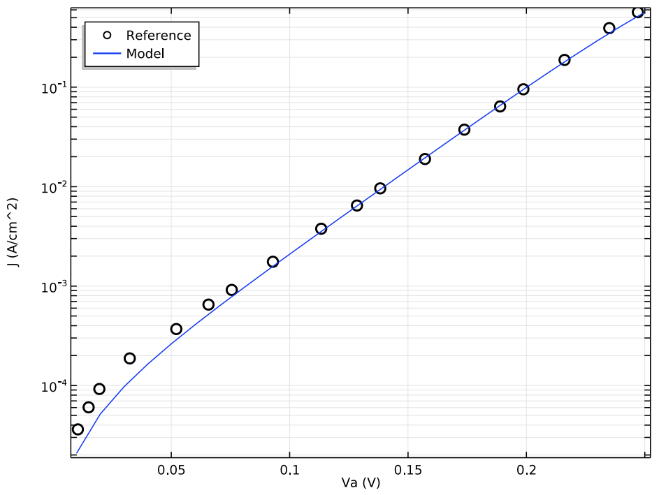
You can keep the model simple by using the “ideal” Schottky contact. This means that you can calculate the current traveling between the materials without accounting for factors like force lowering, tunneling, diffusion effects, and surface states. This type of contact is defined mainly by the thermionic current, which in turn depends on the applied voltage and current density, plotted below.

Comparison of the model (solid line) and experiment (circles) for the current density in the Schottky diode under a forward bias.
As you can see, the results from this benchmark example are in good agreement with experiments, demonstrating that you can accurately capture the behavior of the contact in a Schottky diode with COMSOL Multiphysics and the Semiconductor Module.
Next Steps
Get started with modeling Schottky diodes by trying this example for yourself. Click the button below to head to the Application Gallery, where you can find step-by-step instructions. You can also download the MPH file for this model.
Learn more about semiconductor simulation on the COMSOL Blog:


Comments (0)