
As of version 6.0 of the COMSOL Multiphysics® software, in the Semiconductor Module, we have introduced the optional contribution of contact resistance to the Metal Contact boundary condition of the Semiconductor physics interface. In this blog post, we discuss a benchmark model of a cross-bridge Kelvin resistor that takes advantage of this new functionality.
Model Structure
Cross-bridge Kelvin resistor structures are commonly used to characterize the contact resistance of metal–semiconductor contacts. Here, we examine a specific series of test structures described in Ref. 1.
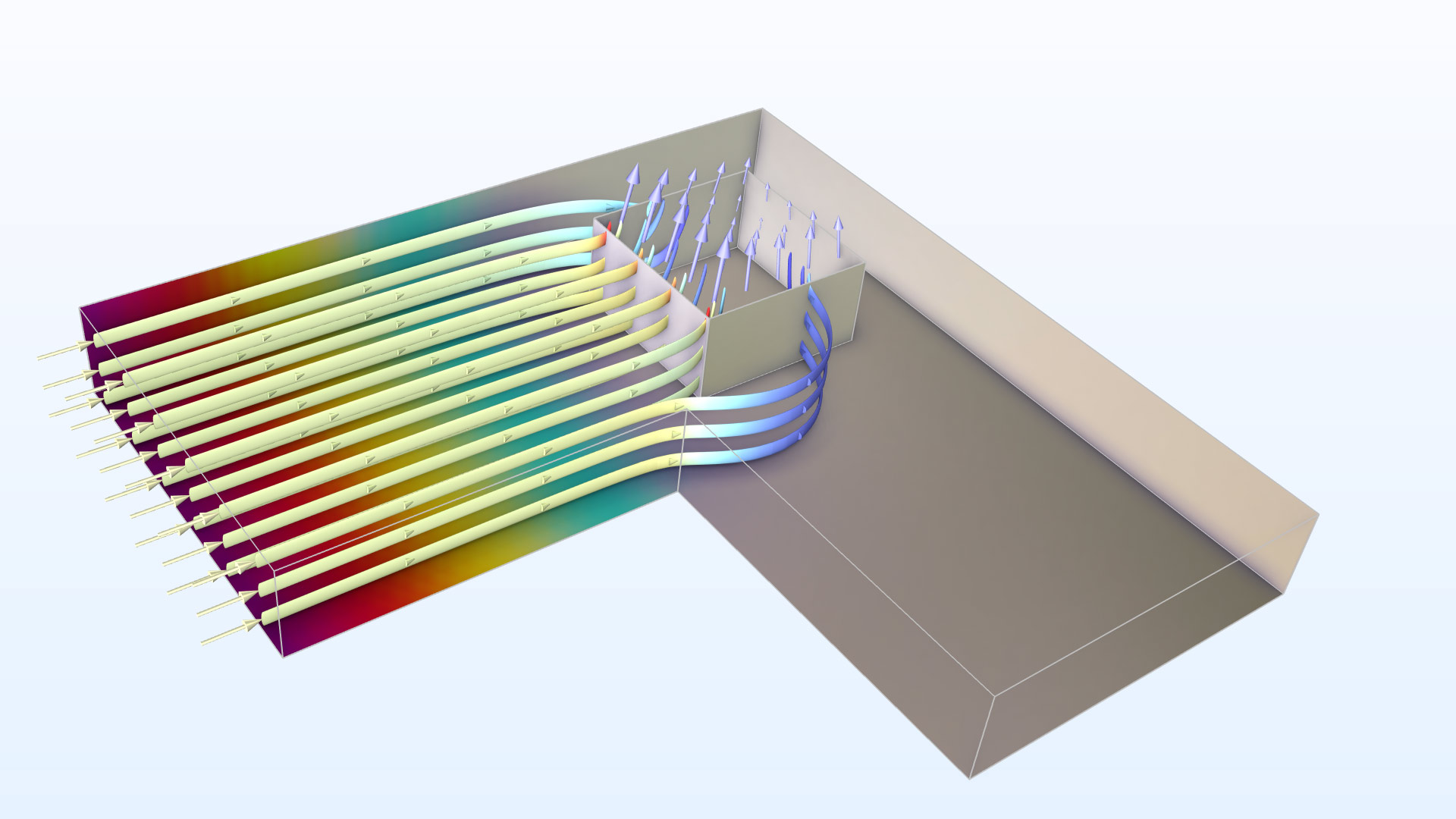
A simulation of the electric potential (color) and current density (arrows and streamlines) of a cross-bridge Kelvin resistor for contact resistance measurement.
The heart of the structure is a 5000 Å thick n+ doped polysilicon layer that is patterned to an “L” shape, as shown in the sketch above. Current is injected into the left arm of the “L” and exits through a square contact window to a metal layer above, as indicated by the arrows (the metal layer is not shown explicitly in the sketch). A bridge voltmeter measures the voltage drop between the right arm of the “L” and the metal layer.
The structure yields a directly measurable quantity, the Kelvin contact resistance R_c (SI unit: Ω), which is obtained by dividing the voltage drop by the total current flowing through the contact window. However, this resistance value is not a good quantity for characterizing the contact, because it will change depending on the dimensions of the test structure. This is due to the to the nonuniform distribution of the current density through the contact window (the current crowding effect, as shown by the varying lengths of the arrows in the sketch above).
The nature of the metal–semiconductor contact is better characterized by another quantity, the specific contact resistivity \rho_c (SI unit: Ω m2), which is defined as the local voltage drop divided by the normal current density within an infinitesimal contact area element. This quantity cannot be measured directly and must be extracted from the measured R_c value using numerical simulation.
Extracting the Specific Contact Resistivity
Ref. 1 reported two series of measurements of the value of R_c as the dimensions of the test structure are varied. In the first experiment, the size of the contact window (l) is varied from 5.0 to 65 μm, while the width of the two arms of the “L” (the diffusion tap width, w) is maintained 5 μm larger than l. In the other experiment, the diffusion tap width w is varied from 7.5 to 60 μm, while the contact window size l is kept constant at 5 μm. The R_c–l and R_c–w data generated from these experiments can be used to extract the specific contact resistivity \rho_c, by running numerical simulations with different values of \rho_c and looking for the best fit between the experimental data and the simulated R_c–l and R_c–w curves.
The authors of Ref. 1 opted for a 2D approximate model for the numerical simulation. The 2D model is described in detail in Ref. 2. In brief, starting from a 3D model, similar to the one provided by the Semiconductor Module, the Schottky band bending and minority carrier effects are ignored (assuming ideal ohmic contact), and only the majority carrier is considered. The conductivity of the metal is much higher than the semiconductor, thus the electric potential within the metal is assumed to be uniform over the entire contact window.
Approximate 2D Model
To simplify the 3D model to an approximate 2D model, the conductivity of the semiconductor is assumed to be uniform in the in-plane directions, and the thickness-direction dependence of the conductance is lumped to one single parameter R_s, the sheet resistance (SI unit: Ω). Under the assumptions that the metal is grounded and the transfer length l_t (\equiv\sqrt{\rho_c/R_s}, SI unit: m) is larger than the thickness of the n+ doped layer, a simple 2D equation can be derived for a new variable, the conductivity weighted average potential V_{2D} (SI unit: V). The equation is
(1)
under the contact window, and
(2)
elsewhere.
The subscript t of the Laplacian operator denotes the in-plane (tangential) directions. For this 2D model, the in-plane current density can be evaluated as
(3)
and the normal current density through the contact window is given by
(4)
In the tutorial example, both the 3D and 2D models are built and the results are compared.
3D Model Setup
The 3D model is straightforward to set up using the Semiconductor interface, with the Contact resistance option enabled for the Metal Contact boundary condition at the contact window.
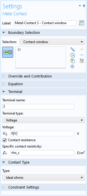
The Contact resistance option is activated for the contact window.
For the terminal on the left, instead of a current input, a small voltage V0 is applied for easier convergence. The input current can be easily evaluated after solving using a built-in variable. For the terminal on the right, the bridge voltmeter is assumed to have infinite impedance, so a zero current boundary condition is applied to the metal contact, and the measured voltage drop corresponds to the terminal voltage after solving.
A swept mesh is used as required by the default finite volume discretization. The mesh is parameterized such that the resolution around the perimeter of the contact window is maintained when sweeping the dimensions of the test structure.
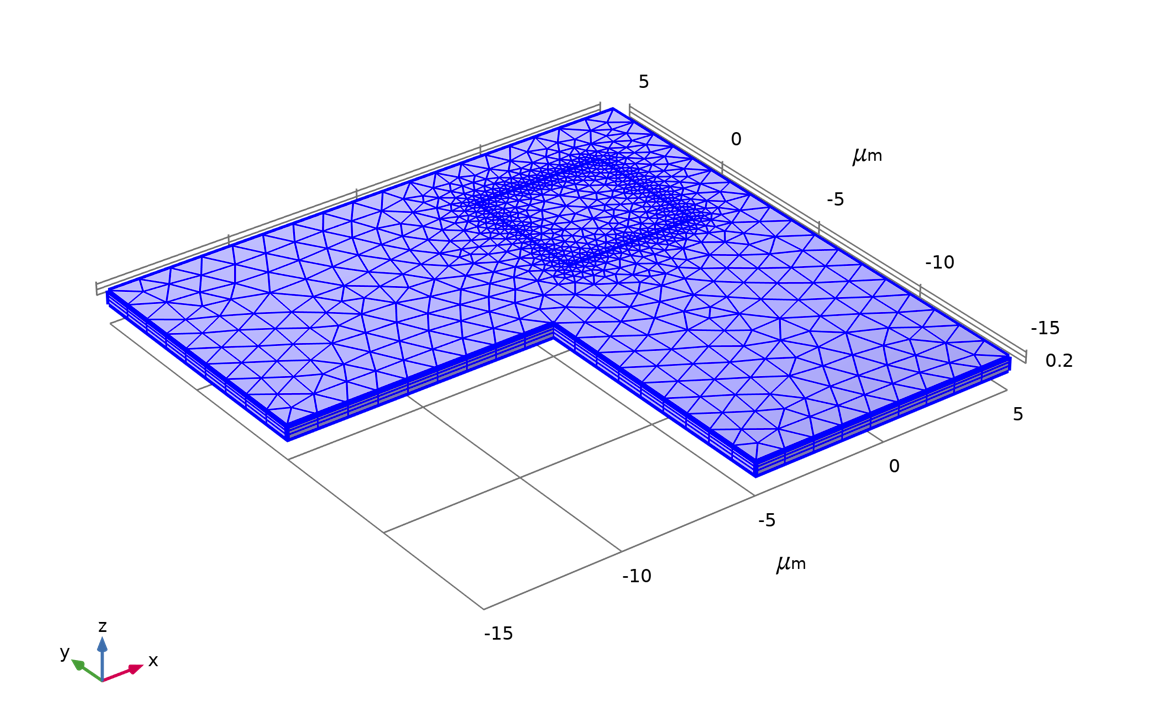
An example of the mesh used in the model.
2D Model Setup
The 2D model with the customized equations 1 ~ 4 is simple to create using the General Form Boundary PDE mathematical interface, on the top surface of the same geometry used for the 3D model. Since this mathematical interface “lives” on the surface, a “domain” is a 2D surface and a “boundary” is a 1D edge. The dependent variable is named V2D to represent the variable V_{2D} in the equations.
The left-hand side of equations 1 and 2 are identical and can be implemented using the default General Form PDE domain condition, with the minus signs removed from the default expressions for the Conservative Flux, and the Source Term and Damping Coefficient set to zero to match the left-hand side of the equations, as shown in the screenshot below. (The conservative flux vector {V2DTx,V2DTy,V2DTz} represents the tangential gradient of the conductivity-weighted average potential \nabla_t V_{2D}.)
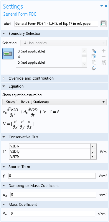
Settings window for the default General Form PDE domain condition.
For the right-hand side of equation 1, add a Source domain condition at the contact window and enter the expression V2D/lt^2 for the Source Term input, corresponding to the formula \frac{V_{2D}}{l_t^2} for the right-hand side.
Apply the same small voltage V0 to the left terminal as in the 3D model, using a Dirichlet Boundary Condition. To obtain an accurate current density based on equation 3, enable the Use weak constraints check box. This instructs the software to create and solve for the Lagrange multiplier V2D_lm on the boundary. We can use it to compute the normal input current density using the expression V2D_lm[V/m]/Rs, corresponding to the formula given in equation 3. The total input current at the terminal can then be computed by integrating the current density over the boundary using an integration operator.
For the right terminal, also apply a Dirichlet Boundary Condition with a weak constraint, now with an unknown applied voltage V2D_ode. Add a Global Equations node to solve for the unknown V2D_ode, such that the terminal current is zero (assuming the impedance of the bridge voltmeter is infinite as in the 3D model). The terminal current is computed from the Lagrange multiplier in a similar fashion to the left terminal.
Finally, the expression for the normal current density flowing out of the contact window is simply V2D/rho_c, as given by the formula in equation 4.
Study and Results
Following the two series of experiments in Ref. 1, two studies are created to vary the contact window size l and the diffusion tap width w using a parametric sweep. (Note that an auxiliary sweep cannot be used to vary the geometry or mesh).
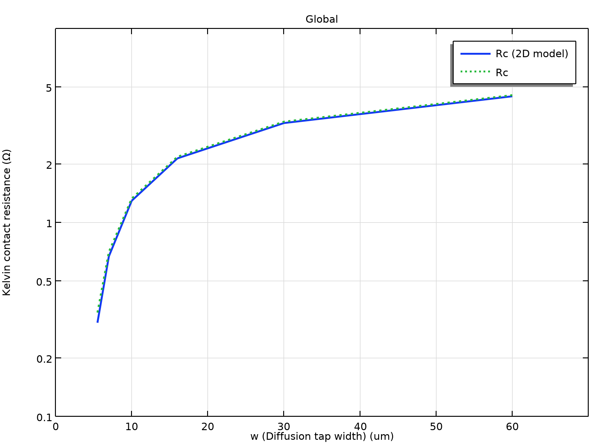
Using the best-fit value for the specific contact resistivity \rho_c (4.5e-8 Ω cm2) as an input to the model, the simulated Kelvin contact resistance R_c is plotted against the contact window area l^2 and the diffusion tap width w in the two plots below.
Simulated Kelvin contact resistance R_c versus the contact area l^2 and the diffusion tap width w. Solid curve: 2D model; dotted curve: 3D model.
We see that the 2D and 3D models give very similar results and agree well with the figures in the paper.
Concluding Thoughts
In this blog post, we illustrate the use of the Contact Resistance feature for the Metal Contact boundary condition. We also show how easy it is to perform equation-based modeling using a built-in mathematical interface. Let us know how you take advantage of this flexibility and versatility of COMSOL Multiphysics for your simulation work in the comments below!
Try It Yourself
Try modeling a cross-bridge Kelvin resistor for the extraction of a specific contact resistivity yourself by clicking the button below, which will take you to the Application Gallery and a downloadable MPH file:
References
- W. M. Loh, S. E. Swirhun, E. Crabbe, K. Saraswat and R. M. Swanson, “An accurate method to extract specific contact resistivity using cross-bridge Kelvin resistors”, IEEE Electron Device Letters, vol. 6, no. 9, pp. 441–443, 1985, doi: 10.1109/ EDL.1985.26185.
- W. M. Loh, S. E. Swirhun, T. A. Schreyer, R. M. Swanson and K. C. Saraswat, “Modeling and measurement of contact resistances”, IEEE Transactions on Electron Devices, vol. 34, no. 3, pp. 512–524, 1987, doi: 10.1109/T-ED.1987.22957.




Comments (1)
Behzad Namvar
July 15, 2022Hi,
Does your model consider the dependence of the contact resistance to the temperature? Because I did not see any expression for temperature dependence!
And if so, what is the temperature range that it can simulate? Does it cover the cryogenic temperatures?