
A Gaussian beam that is striking an array of nanorods is an example of optical scattering. Consider metallic nanorods that are very close together and have a diameter much smaller than the wavelength of a Gaussian beam that falls upon them. If the beam were to be polarized along the rods, they would act as though they were not actually individual rods, but a sheet of metal. The array is nearly transparent to the wave when it is polarized perpendicular to the rods.
What a Gaussian Beam Is
Before digging further into this example, let’s make sure we understand what a Gaussian beam is. In short, it is an electromagnetic beam where a Gaussian function can be used to describe the electric field profile in a plane that is perpendicular to the axis of the beam. Most lasers emit a beam that very nearly approximates a Gaussian beam, thus it occurs often when analyzing photonic devices. If you want to learn more about modeling Gaussian beams, please check out the following models in the Model Gallery:
- Second Harmonic Generation from a Gaussian Beam
- Splitting of a Gaussian Beam
- Self-Focusing of a Gaussian Beam
- A Gaussian beam passing through a metamaterial lens
Modeling Optical Scattering in Nanorods
Now, let’s get to our optical scattering example. Suppose we want to investigate whether or not there is electromagnetic coupling between the nanorods in an array. In theory, we know that under the right conditions there will be coupling — by modeling the phenomenon, we can verify that it really is the case.
Assume we have a Gaussian beam with a 750 nm wavelength and a spot radius of equal length. We also have an array of 40 metallic nanorods, each with a radius of 20 nm. I mentioned in the beginning that the rods are very close to each other; to be precise, the separation between the rods is only 150 nm. The tightly focused beam is striking the nanorods, and propagates in the negative y-direction.
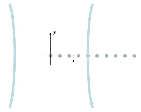
Gaussian beam incident on an array of nanorods.
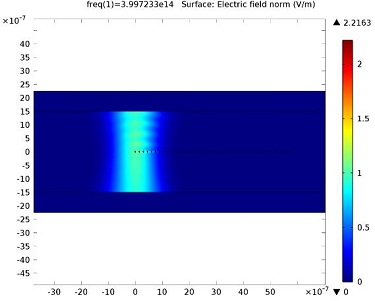
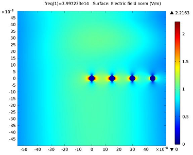
In order to get an idea of the coupling, we can set up and solve for this model using COMSOL Multiphysics and the Wave Optics Module. As you can see in the image above, only a few of the nanorods are illuminated by the electromagnetic beam. By setting up a surface plot, we can visualize the beam’s electric field norm when it’s polarized in the grating vector direction (the x-direction). Below to the left, you can see that half of the beam is illuminated by the nanorod array, and there is no noticeable reflection or diffraction. If you want a closer look at the rods, you can create a second, zoomed-in version of the surface plot (below, right). This demonstrates that there is dipolar coupling between the rods.
|
|
Electric field norm surface plot when the beam is polarized in the x-direction. |
Close-up of the nanorods, showing dipolar coupling. |
As you can see in the line graph below, the coupling extends much farther than the light beam’s intensity distribution.
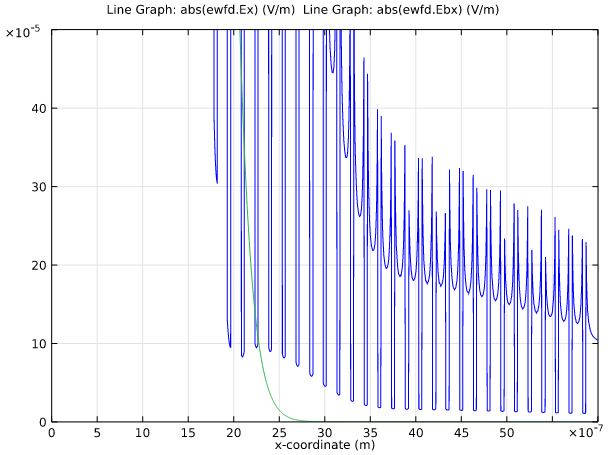
Graph of the electric field’s x component (blue) and the background field of the beam (green). The
beam is polarized in the x-direction.
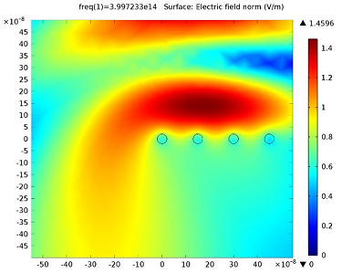
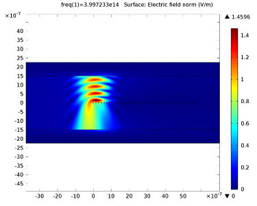
We can also plot a close-up of the beam as polarized in the z-direction instead of in the direction of the vector grating. Doing so will illustrate a scenario where the nanorod array behaves like an opaque metal sheet to the beam, reflecting the beam and causing strong edge diffraction. This effect is clearly demonstrated in the bottom-right plot.
|
|
| Close-up of the nanorods when the beam is polarized in the z-direction, causing the array to act like an opaque metal sheet rather than individual rods. | Reflection and edge diffraction effects. |
Nanorod Applications
The main intended application of the model outlined here is short-range optical communication, where light follows the path laid out by the array of nanorods. As the nanorods are smaller than the wavelength of light, and light is tightly coupled to the nanorods, the width of the light path is narrower than the wavelength. Therefore, this technology could open up for spatially dense optical communication channels, for instance between electrical circuits on chips and printed circuit boards.
You may have also heard about nanorods in a different context. In addition to what is demonstrated in this modeling example, nanorods can be used in cancer treatment.


Comments (0)