
Traps are omnipresent in practical semiconductor devices. When modeling these devices, the Trap-Assisted Surface Recombination boundary condition adds the effects of charging and carrier capturing/releasing by surface or interface traps. Here, we examine a tutorial model of a metal-oxide-silicon capacitor (MOSCAP) to demonstrate how to use the feature in the Semiconductor Module, an add-on product to the COMSOL Multiphysics® software.
About the Trap-Assisted Surface Recombination Boundary Condition
The Trap-Assisted Surface Recombination boundary condition adds contributions to the surface recombination rate and the surface charge density associated with the surface traps for the Insulation, Thin Insulator Gate, Insulator Interface, and Metal Contact (Ideal-Schottky-type) boundary conditions. This feature replaces and expands the functionality of the Surface traps check box found in versions prior to the COMSOL® software version 5.4. Both the Shockley-Read-Hall model and the Explicit trap distribution options are available.
Modeling a MOSCAP
The MOS structure is an essential element of numerous silicon planar devices. Therefore, we have included a few MOSCAP tutorial models in the Application Gallery for the Semiconductor Module. Here, we use the MOSCAP 1D Interface Trap model to showcase the trap-assisted surface recombination feature.
As the name suggests, it is a simple 1D model of a MOSCAP including the effects of interface traps. The model is based on the experimental device (the n-type sample) described in Fig. 14 of a paper by E.H. Nicollian and A. Goetzberger (Ref. 1).
The experimental samples were prepared with a 10-um-thick epitaxial (epi) layer grown on low-resistivity substrates to minimize the effect of the bulk series resistance. In the model, the epilayer is assumed to be the same thickness (10 um), and the substrate is 2 um thick, assuming that the bulk series resistance can be ignored. The oxide thickness is assumed to be 60 nm, which is in the middle of the experimental range of ~50–70 nm. The diameter of the gate is 3.8×10⁻² cm, as given in the figure caption in the paper.
The electron mobility is assumed to be constant at 1450 cm2/V/s. The n-doping concentrations in the epilayer and the substrate are then computed from the experimental values of resistivity of 0.75 and 0.005 ohm-cm, respectively.
The oxide dielectric constant is assumed to be 3.9. The oxide capacitance is then computed from the dielectric constant, thickness, and gate diameter.
The fixed oxide charge density is 9×1011 cm-2, as given by the paper. This value is included in the model in addition to the trap charges.
The trap energy distribution is assumed to be rectangular with a range of 0.2 eV, centered around the midgap. The height of the rectangle is assumed to be 2×1011 cm-2eV-1, as suggested by Fig. 15 of the paper. For the capture process, the thermal velocity is assumed to be 107 cm/s, and the cross sections are 1×10-15 cm2 and 2.2×10⁻¹⁶ cm2 for the electrons and holes, respectively, as given on the same page as Fig. 15.
The metal work function of the gate is assumed to be 4.5 eV.
Setting Up the Trap-Assisted Surface Recombination Boundary Condition
By default, the trapping model for the boundary condition is the Shockley-Read-Hall model. For this tutorial, which has a rectangular trap energy distribution, we instead choose the Explicit trap distribution option. Then, under the Trapping section, choose the Specify continuous and/or discrete levels option. These settings are shown in the screenshot below.
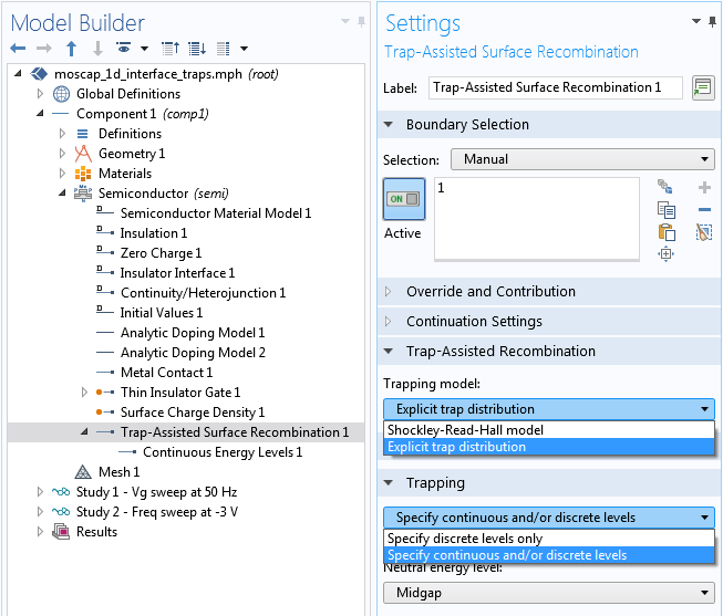
Setting the trapping model and the trap energy level options.
The Explicit trap distribution option requires one or more subnodes to specify the distribution of the trap energy level(s) in order for the boundary condition to take effect. Here, we add the Continuous Energy Levels 1 subnode.
The continuous trap energy distribution is approximated by a number of discrete levels along the energy axis using the extra dimension functionality of the software. We can make more efficient use of the extra dimension by shrinking the range of discretization to be the same as the one for the rectangle distribution. This is shown in the screenshot below; for example, setting the Continuous energy discretization, min energy (the Et,min input field) to semi.tasr1.ctb1.Et0-Ew0/2.
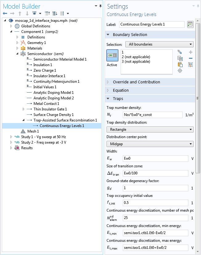
Setting up the continuous trap energy distribution.
Examining the Semiconductor Simulation Results
The experiments described in the paper measure the small-signal response of the samples; therefore, we also perform a small-signal analysis of the model. The figure below shows the computed terminal capacitance and the equivalent parallel conductance as functions of the gate voltage to compare with Fig. 23 in Ref. 1. The curves show the same qualitative behavior with comparable magnitudes as the experimental data (note the peaking of the equivalent parallel conductance and the wiggle of the terminal capacitance).
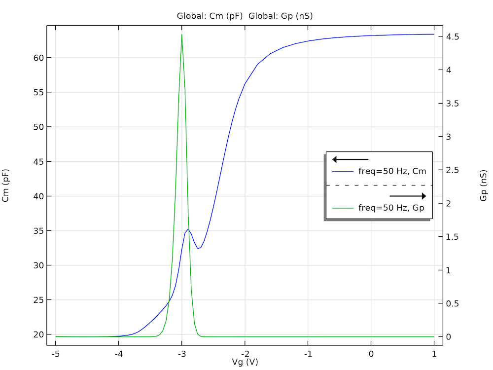
The computed terminal capacitance (Cm) and equivalent parallel conductance (Gp) as functions of the gate voltage (Vg) show the same qualitative behavior with comparable magnitudes as the experimental data reported in the paper.
The figure below shows the computed terminal capacitance and the equivalent parallel conductance as functions of the small-signal frequency. The qualitative behavior of the equivalent parallel conductance compares well with Fig. 25 in the paper (the figure did not include the terminal capacitance).
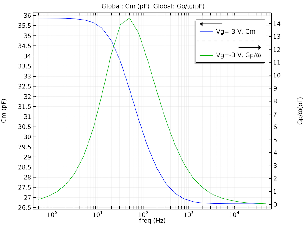
The computed terminal capacitance (Cm) and equivalent parallel conductance (Gp) as functions of the small-signal frequency.
Gaining Insight into the Physics of Interface Trapping
One of the benefits of simulation is to help us understand the system better by investigating numerical quantities that are not accessible to experiments. In this model, we can plot the simulated trap occupancy along the energy axis to gain insight into the behavior of the measured capacitance and conductance curves, as exemplified by the images above.
The energy axis is added to the model by the physics interface using an extra dimension component, as mentioned above. To plot any quantity along the energy axis, we first create a dataset pointing to the extra dimension component where the quantity is defined. This is easily done by duplicating the dataset of interest and then choosing the extra dimension option in the Component drop-down menu, as shown in the screenshot below.

Creating a dataset to plot quantities along the energy axis.
In addition to the dataset, the expression to be plotted requires the use of the atxd operator, which helps evaluate quantities in the extra dimension (along the energy axis). For example, the following screenshot shows the expressions for the y-Axis Data and the x-Axis Data for a line graph. The operator atxd0 is used with a “0” because the energy axis (extra dimension) is defined in a boundary condition, which has a dimension of 0 in the 1D model. The first argument for the operator is 0[um], since the boundary condition is applied on the boundary located at 0 um in the model geometry.
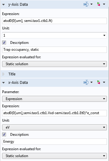
The expressions for the line graph’s y– and x-axis data.
The figure below shows the steady-state (the bias point) trap occupancy along the energy axis for two cases:
- Gate voltage = 1 V (accumulation)
- Gate voltage = -3 V (peak of equilibrium parallel conductance)
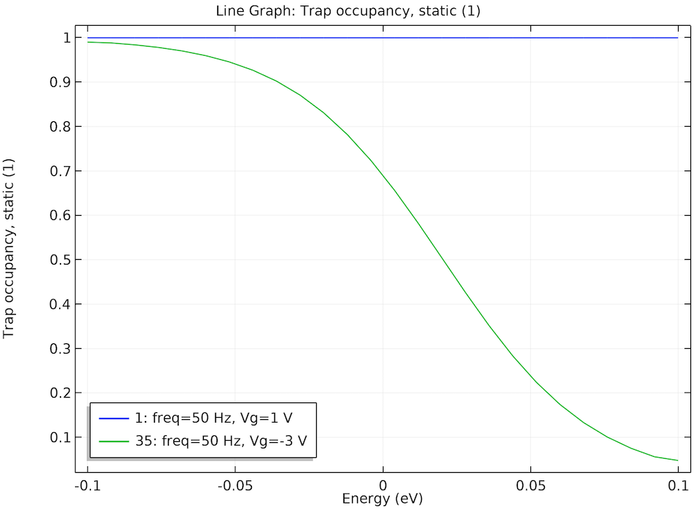
Steady-state trap occupancy at two bias points offers insight into the behavior of the computed terminal capacitance and equivalent parallel conductance curves.
Since the Fermi level is far above the trap energy levels, we see that at the gate voltage of 1 V, the traps are fully occupied (blue curve). In this case, we would not expect any significant contribution to the small-signal response from the traps. However, at the gate voltage of -3 V, the Fermi level goes through the middle of the trap energy distribution, so many trap levels are partially occupied (green curve). In this case, we would expect the traps to contribute significantly to the small-signal response. This is indeed consistent with the peaking of the equivalent parallel conductance and the distinct wiggle of the terminal capacitance curve at -3 V seen in the earlier figure.
The figure below shows the small-signal response of the trap occupancy along the energy axis and compares the same two cases: gate voltage = 1 V (accumulation) and gate voltage = -3 V (peak of equilibrium parallel conductance). Since the small-signal response is complex valued, we plot both the real part (in solid curves) and the imaginary part (in dashed curves).
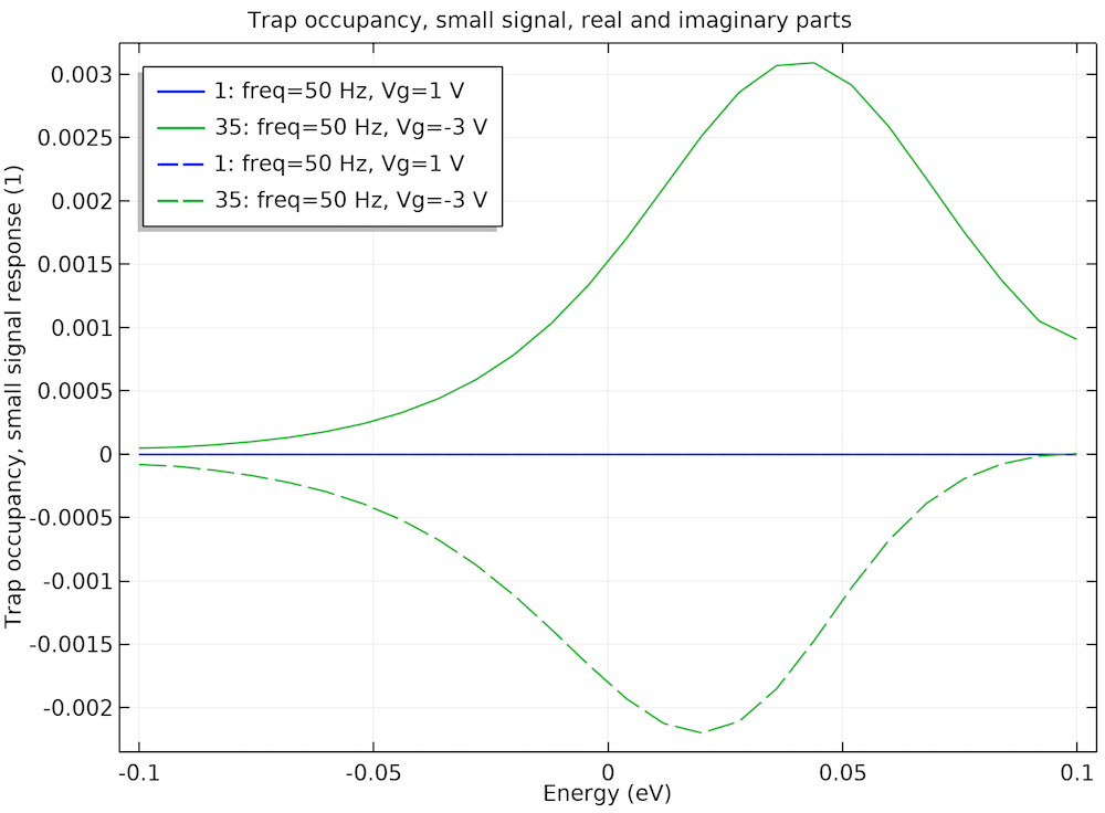
Small-signal response of trap occupancy at the same two bias points further confirms the previous observation. Solid curves: real part; dashed curves: imaginary part.
On one hand, we see that at the gate voltage of 1 V, both the real and imaginary parts of the small-signal response of the trap occupancy are very small (blue curves). On the other hand, at the gate voltage of -3 V, both the real and imaginary parts of the small-signal response of the trap occupancy are significant (green curves). All of these provide further confirmation for the physical argument given above.
Next Step
In this blog post, we have showed that the Trap-Assisted Surface Recombination boundary condition adds the essential effects to a model of a semiconductor device in order to reproduce the qualitative behaviors of experimental data found in the literature. We have also showed how to plot quantities in the extra dimension, such as the energy axis in the model.
To try the Interface Trapping Effects of a MOSCAP tutorial model yourself, click the button below to go to the Application Gallery, where you can download the PDF documentation with step-by-step instructions and the MPH file for this tutorial.
We hope you find this feature useful and we would love to hear how you apply it to your research.
Reference
- E.H. Nicollian and A. Goetzberger, “The Si-SiO2 interface – electrical properties as determined by the metal-insulator-silicon conductance technique” The Bell System Technical Journal, vol. 46, issue 6, Jul./Aug. 1967).


Comments (0)