
Simulation of 3D semiconductors has the potential to be extremely useful when developing and improving semiconductor technology by reducing the amount of experimentation and fabrication required to design complex devices. Modeling 3D devices is challenging as the length scales that must be resolved, combined with the nonlinear nature of semiconductor physics phenomena, often require computationally expensive simulations. Here, we share an example simulation of a 3D bipolar transistor and important advice for effective modeling of 3D semiconductors with COMSOL Multiphysics.
Bipolar Transistors
Originally invented in the late 1940s, bipolar transistors were widely used in the first integrated circuits. Although modern field-effect devices have largely replaced bipolar transistors in digital logic circuits, bipolar transistors remain widely used for analog applications. They are particularly widespread in power regulation circuitry, where they are used as switches and current amplifiers.
Simulation Considerations
In order to ensure that a simulation effectively captures all the required physics to give an accurate result, it is important to understand the processes that need to be included in the model. These could vary depending on the configuration of the device and the situation in which it is intended to operate. It is always a good idea to ensure that a model gives satisfactory reliability and accuracy while minimizing the complexity of the problem.
This is particularly important for 3D semiconductor simulations, where models created using non-recommended techniques can take many days to solve or possibly never converge.
In this blog post, I will walk you through the process for setting up a 3D semiconductor model of a bipolar transistor device. First, I will introduce and explain the operation of the device and the important physical processes that must be included. I will also discuss the measures needed to effectively include them within the model.
Doping Structure and Device Symmetry
Like many semiconductor devices, doping is critical to the operation of bipolar transistors. There are two kinds of doping: p-type doping, where a region has extra holes, and n-type doping, where a region has extra electrons.
A bipolar transistor consists of three regions of alternating p-type and n-type doping. Although there are two possible doping structures, n-p-n or p-n-p, we will focus on the n-p-n configuration as this is the most common variety. The n-p-n structure is formed by sandwiching a p-type layer between two n-type layers. The device can be considered to have three different regions known as the emitter, base, and collector. Each region can be individually electrically addressed via three separate metal contacts, which are labeled according to the region that they are connected to.
A schematic of the n-p-n doping structure, device regions, and electrical connections is shown here:
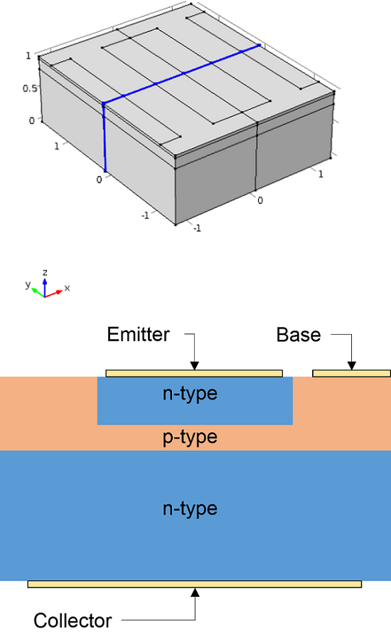
Geometry and structure of the bipolar transistor device. Top: The geometry of a bipolar transistor device represented in the COMSOL Multiphysics simulation software. Bottom: Cross section through the device taken along the z-x plane, highlighted by blue edges in the upper image. The n-p-n doping pattern is labeled, along with the electric contacts that connect to the emitter, base, and collector regions.
Due to the alternating doping of the three regions, the bipolar transistor forms two back-to-back p-n junctions that share the base region. The behavior of carriers as they encounter these p-n junctions is crucial for the operation of the bipolar transistor.
Throughout the rest of this example modeling process, I will present suitable steps for including all the relevant physics needed to describe this behavior in a computationally efficient way.
Planes of Symmetry
The first question to ask yourself when designing a 3D semiconductor model is: “Can I use symmetry to reduce the model size?”
Many kinds of devices have planes of symmetry, rotational symmetry, or even axisymmetric geometry. If at all possible, using axisymmetric designs is recommended, as this can reduce a 3D simulation down to 2D. An example of the axisymmetric modeling of a cylindrical field-effect transistor can be found here.
The device we want to model in this example has two planes of symmetry that bisect the device in the x-z and y-z planes. This means that we only need to model one quadrant. In the figure below, the upper-right quadrant has been selected:
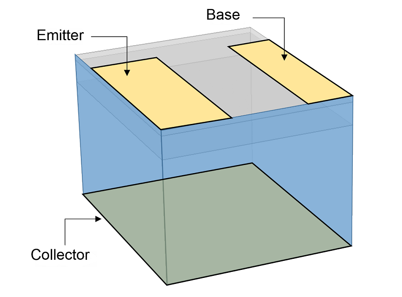
Geometry required by the model. Due to the planes of symmetry, which are highlighted in blue, only one quadrant of the entire device needs to be included. This reduces the size of the model, allowing it to be solved in a shorter amount of time and with less memory. The metal contacts are applied to surface boundaries as indicated.
Ensuring that Doping Profiles Are Resolved
After creating the smallest model geometry that symmetry allows, the next question for consideration is: “What resolution do I need to reliably capture the physics within the model?”
Obviously, the geometry dimensions of the device need to be sufficiently resolved. However, the required physical processes often take place on a length scale that is much smaller than the geometry features. For semiconductor models, ensuring adequate resolution can be a challenge, as the various physical processes that are involved often require very different length scales. To make things more complicated, the spatial resolution required to adequately describe many processes can vary drastically throughout the device and can even vary as a function of other model parameters, such as the applied voltages.
A good place to start is to ensure that the doping profiles are resolved. This is because in regions where the dopant concentration changes rapidly, other quantities often undergo drastic variation as well. Thankfully, ensuring that the doping profiles are resolved is relatively straightforward, as the dopant distribution is user-controlled and does not vary when other model parameters change.
The COMSOL Multiphysics simulation environment provides convenient tools for easily viewing the doping throughout devices. It is a good practice to use the Get Initial Value option available from the Study node, since the dopant concentration is an analytic function that can be computed and visualized without solving the semiconductor equations. The initial value of the doping can then be plotted to help set up a suitable mesh for the full computation.
Below, I have added a 3D volume plot of the doping throughout the model, along with a line cut of the dopant concentration taken along a vertical cut through the center of the device.
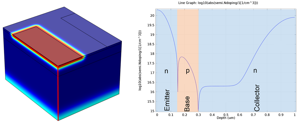
Dopant distribution throughout the bipolar transistor device. Left: 3D visualization of the doping throughout the model geometry. The red area in the front-top corner is the n-type emitter region. Due to the order of magnitude variation in the dopant concentration, which is typical of semiconductor devices, it is difficult to see the three different doping regions. Right: Line cut of the dopant concentration taken along the red line in the left-hand image. The logarithmic scale allows the n-p-n doping pattern to be clearly seen and each region is labeled. Note that the dopant concentration varies within each region but the most rapid changes in dopant concentration occur around the emitter-base and collector-base p-n junctions.
Creating an Effective Mesh
In COMSOL Multiphysics, it is advantageous to use a structured swept mesh for 3D semiconductor simulations. This is where a surface mesh on an exterior face of the geometry is swept through the geometry volume, resulting in mesh elements that are prisms aligned with the direction of the sweep.
This can be seen in the mesh used in our example model, shown below, where a free-triangular mesh has been generated on the top surface and then swept down to the bottom surface. The mesh is structured so that the height of the prisms vary throughout the device, tightening the mesh in the z-direction in regions that require high resolution.
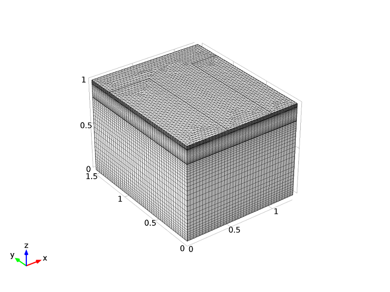
The mesh used is a structured swept mesh where the resolution in the z-direction is largest around the p-n junctions and near to the electrical contacts on the top and bottom surfaces.
As discussed above, it is important to refine the mesh around gradients in the doping profile. This has been achieved by using an extra geometry cuboid embedded within the main device domain just under the top surface. The extra cuboid is positioned such that the extra internal boundaries are in regions where the dopant concentration gradient is largest. These internal boundaries are used to control the structure of the mesh to tighten it in the required regions. Additionally, for semiconductor models, it is a good idea to tighten the mesh near electrical contacts in order to resolve the high current densities and electric field effects that are often present in their vicinity. For this reason, the mesh has also been refined near the top and bottom surfaces of the device.
Refining the mesh around doping gradients and near electrostatic boundaries is a good starting point. However, as mentioned earlier, care must be taken to consider the physical processes that are present in the model and modify the mesh to accommodate them.
For the bipolar devices modeled here, the active areas are spread over the p-n junction regions and there are no other special length scales to consider besides ensuring that the p-n doping structure is resolved. However, other devices may need additional thought. For example, field-effect devices often require very fine meshing under surface gate contacts, as the current density is localized very drastically in the thin channel regions under these gates (see here).
When in doubt, a good quantity to consider is the Debye length, which is smallest in regions that have high charge density. Finally, as with any numerical simulation, it is important to assess COMSOL Multiphysics models to ensure that solutions are mesh independent. You can achieve this conveniently by parameterizing the mesh density and varying the parameter using an auxiliary sweep.
For 3D semiconductor models, it is advisable to perform some preliminary studies to confirm a suitable mesh resolution before moving on to creating the full model. For example, you could simulate a 2D cross section to get an idea of the Debye length and to test for mesh independence prior to progressing to a full 3D version.
Capturing Relevant Physics
Semiconductor devices can often be operated in a variety of different configurations depending on the intended application. As 3D semiconductor simulations are computationally intensive, it is advisable to carefully consider the relevant application and design the model to compute suitable solutions.
When building a semiconductor model in COMSOL Multiphysics, it is useful to ask yourself: “What physics is important for my device?”
For 3D semiconductor models, including additional physical effects rapidly increases the computation time, so try to limit the model to only the important processes. For example, when modeling a device where the vast majority of current is carried by electrons and holes do not significantly participate, it may be suitable to solve only for electrons rather than both electrons and holes. Alternatively, when modeling a device that is connected to a very effective heat sink, it is perhaps not important to simulate the effects of varying temperature.
Below is a screenshot of the Model Builder for our bipolar transistor example model. In addition to the default nodes, the doping structure has been created using three domain features and the contacts have been assigned to the appropriate boundaries using boundary features. A Trap-Assisted Recombination feature has also been added, as this is needed to correctly account for the current flow through such a highly doped device. However, no other physical processes are included.
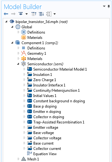
Model Builder for the example bipolar transistor model.
Current Amplification for Sensing Circuitry
A common operation mode for bipolar transistor devices is for the emitter to be grounded and for voltages to be applied individually to the base and collector regions. This configuration, which is shown in the figure below, is suitable for using the bipolar transistor as a current amplifier. We will model this configuration.
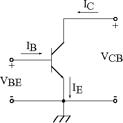
Circuit diagram showing a bipolar transistor in the common emitter configuration.
The Importance of Minority Carriers
This operation mode results in both the base and collector voltages being measured relative to the grounded emitter, so this set-up is known as the common emitter configuration.
In the common emitter configuration, the effective resistance between the emitter and collector can be varied by applying a current to the base. This enables the device to function as a current amplifier. This is because the magnitude of the current that flows between the collector and emitter (at a given collector-emitter voltage) is proportional to the current that flows between the base and the emitter.
The ratio between the current that is output from the collector to the current that is applied to the base is known as the current gain. Typical bipolar transistors have current gains of over 100, enabling the current output from the collector to be controlled by an input base current that is over 100 times smaller than the required output current. This makes bipolar transistors attractive across a broad range of power management applications.
A popular application is to use a small current from some sensing circuitry to control the current flow to a more energy-intensive component. For example, a small current produced by a temperature-sensing circuit can be used as an input to control a larger output current needed to power a heating element. With a particular chosen application, we can consider the relevant physical processes to ensure that our model includes the correct features and is adequately resolved.
Bipolar transistors get their name from their reliance on both electron and hole currents in order to function. This is in contrast to unipolar transistors, such as common MOSFET devices, in which current is carried only by one carrier species. Because of this, it is important to model both electron and hole currents when simulating bipolar devices.
In order to understand the operation of an n-p-n bipolar transistor, it is useful to consider the two p-n junctions that form the device and the direction of the bias that is applied to each one. When used as a current amplifier, the voltage at both the base and collector contacts is positive, relative to the grounded emitter contact, and the voltage at the collector contact has a larger magnitude than that at the base contact. This is known as the forward-active regime.
In the forward-active regime, a forward bias is applied to the emitter-base junction, while a reverse bias is applied to the collector-base junction. The forward bias at the emitter-base junction allows thermally excited carriers to be injected from the emitter into the base region. Electrons that traverse from the n-type emitter region into the p-type base region are referred to as minority carriers, because a p-type region has an abundance of holes but few electrons. The minority carrier electrons diffuse through the base region from a high concentration adjacent to the emitter-base junction towards the lower concentration deeper into the p-type base region. Minority electrons that travel near the reverse bias collector-base junction are then driven to the collector contact by the collector-base junction electric field. However, the majority holes in the base region cannot penetrate the reverse-bias junction. The overall result is that the electron current can flow between the emitter and collector contacts, traversing all three regions, while the hole current is confined to the base and emitter regions.
Assessing the Relevant Physics
Now that we have an idea of how we expect the device to function, it is possible to check if the important physics will be both included in the model and adequately resolved.
We have already refined the mesh around the doping gradient and in the vicinity of the contacts to account for the expected physics common to most semiconductor models. This should ensure that the p-n junctions — and the associated electric fields — are properly resolved. The only additional physical process to consider is the minority carrier diffusion throughout the base region. This is an important physical process, as it significantly affects the performance of the device and could be of interest when designing or optimizing a bipolar transistor.
For instance, the base region must be thin enough compared to the electron diffusion length, so that electrons can make it into the collector region, but not so thin that electrons and holes tunnel directly from the emitter into the collector. As it happens, carrier diffusion is already included in the standard set of semiconductor equations and the mesh is already fairly fine compared to the electron diffusion length in the base region. Therefore, no special amendments are required for this particular model.
Choosing Appropriate Studies and Extracting Results
The last thing to do is to configure suitable studies to simulate the device under conditions relevant to its normal operation. Now is the time to ask yourself: “What are the typical operating conditions for my application?”.
Often, semiconductor devices can be wired up in different configurations for different situations. However, due to computation time considerations, it may not be practical to simulate the full range of possible operational conditions. For example, instead of running a voltage sweep that covers every possible combination of voltages, a study can be restricted to only solve for the combinations and ranges that will be encountered during typical operation.
Furthermore, consider what information is needed from the model and design the studies so that this will be convenient to extract from the solutions. The example model has two studies: one that sets the collector voltage to 0.5 V and sweeps the base voltage and another that sets the base current to 2 μA and sweeps the collector voltage. The first study allows the current gain to be calculated with ease. The second study allows the emitter-collector current to be calculated as a function of emitter-collector voltage for a fixed input base current.
Computing Current Gain
The first study can be used to generate a graph known as a Gummel plot. This is a standard way of evaluating bipolar transistors for use as current amplifiers. It shows the collector and base currents as a function of the base voltage on a logarithmic y-axis scale. The ratio of the collector current to base current gives the current gain, which is a crucial performance parameter for an amplifier device.
Below, you can see a Gummel plot. Judging by the plot, it is clear that the collector current is around two orders of magnitude larger than the base current over the whole base voltage range.
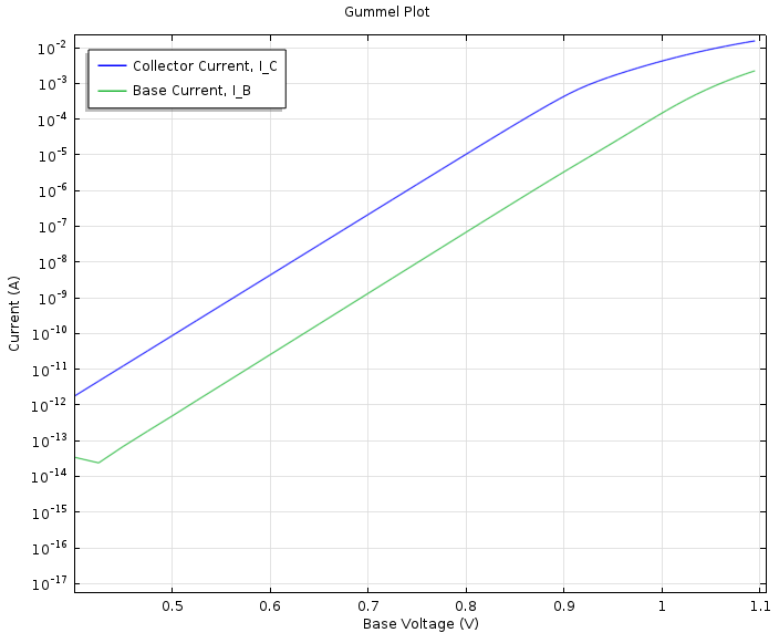
Gummel plot showing the collector and base currents as a function of the base voltage when a voltage of 0.5 V is applied to the collector.
Next, we have a figure that shows the current gain as a function of the collector current. The current gain is fairly constant, at ~160, over a collector current range of 9 orders of magnitude. However, for collector currents above 1 mA, the current gain falls drastically. This simulation indicates that the device has an operational limit of around 1 mA if used as a current amplifier in an application with a collector-emitter voltage drop of 0.5 V.
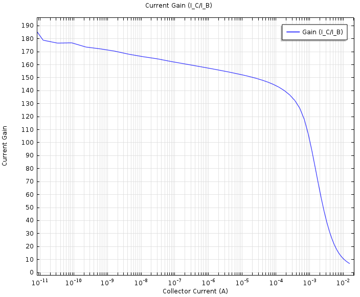
Current gain of the bipolar transistor as a function of collector current with a collector-emitter voltage drop of 0.5 V.
It is important to note that the same study and analysis could be performed at a range of different collector voltages. However, due to the computational expense involved, it is advisable to narrow this range to the expected operational voltages during normal use, as discussed above.
Common Emitter Output Characteristics and Carrier Current Flow
The second study is used to generate a graph of the collector current as a function of collector voltage when an input base current of 2 μA is applied, as shown below. Initially, the collector current increases very quickly with collector voltage, before saturating towards a value of around 300 μA.
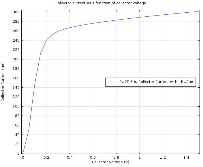
Collector current as a function of collector voltage when an input current of 2 μA is applied to the base.
From 2D simulations of a similar device, it can be shown that the saturation current level is controlled by the input base current. This is an example of when a 2D model can be used in conjunction with a 3D model to make device modeling more efficient. It is a good practice to use a 2D model wherever possible to observe general behavior and identify parameter combinations or ranges of interest before moving to a full 3D device simulation.
Finally, using the full 3D simulation, we can visualize the 3D current flow within the device. The last figure shows arrow plots of the electron current (black arrows) and hole current (white arrows) for a collector voltage of 1.5 V with an input base current of 2 μA, which is in the saturation regime. The color plot slice shows the voltage and allows us to see the p-n junctions. As expected, the hole current does not traverse into the collector region, while the electron current predominantly flows between the collector and emitter.
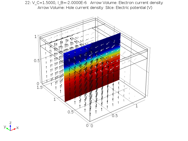
3D visualization of the current flow throughout the bipolar transistor at a collector voltage of 1.5 V with an input current of 2 μA applied to the base. Electron current is shown with black arrows and hole current with white arrows. The color of the slice represents the voltage throughout the device.
Summary of Our 3D Analysis of a Semiconductor Device
This example model demonstrates best practices for modeling and analyzing 3D semiconductors using the COMSOL Multiphysics software. Although the device studied here is relatively simple, the same thought process and model building steps can be applied to any semiconductor model. While 3D semiconductor modeling remains a computationally challenging field, the advice in this blog post should take the guesswork out of getting started and creating useful device models.
Additional Resources
- For more details on the example bipolar transistor models in the COMSOL Multiphysics Model Library, please see:
- For additional information on some of the physics used for this model, please see:
- Informative Wikipedia page on bipolar transistors
- A good general guide to semiconductor junctions


Comments (0)