
Carrier dynamics plays an important role in the transient behavior and frequency response of semiconductor devices. Here, we use two tutorial models of PIN rectifiers in the Semiconductor Module, an add-on to the COMSOL Multiphysics® software, to demonstrate the simulation of dynamical effects.
PIN Rectifier Models in the Semiconductor Module
As of version 5.4 of COMSOL Multiphysics®, two PIN rectifier models are available in the Application Library for the simulation of the transient processes of switching on and turning off power diodes. These processes are referred to as forward recovery and reverse recovery, respectively.
The forward recovery is modeled with an idealized input current profile of a linear current ramp from zero up to a constant-current plateau. During the turn-on time interval with the specified current input, the device voltage shows a temporary spike, due to the finite amount of time required to accumulate extra charge carriers in the drift region for the diode to be fully switched on.
The reverse recovery tutorial uses a more sophisticated model that incorporates the lumped circuit capability of the COMSOL® software to model an inductive load and a flyback diode more realistically. The model also includes band gap narrowing and carrier-carrier scattering effects. For reverse recovery, the diode remains in the forward-biased mode for a short period of time after the applied voltage is switched, due to the large amount of stored charge carriers in the drift region during the on state.
The Forward Recovery Model
The forward recovery tutorial is based on a device model found in Baliga’s book (page 242 in Ref. 1). The structure is 80 um long with a background n-doping of 5e13/cm3 and the peak n- and p-doping at the exterior boundaries being 1e19/cm3. The PIN rectifier, which is current driven, has a constant ramp rate that is 1e9, 2e9, and 1e10 A/cm2/s along with a steady-state current density equaling 100 A/cm2.
The input current profile is specified using a Ramp function with a cutoff. To help the accuracy of the time-dependent solver, the Events interface is used to mark the abrupt change in the slope of the applied current at the end of the current ramp (t_on), as shown in the screenshot below.
![]()
Using the Events interface to mark the time when an abrupt change in the slope of the applied current occurs. Use the Semiconductor Equilibrium study step to solve for the off state as the initial condition for the following time-dependent study step.
Setting Up the Time-Dependent Forward Recovery Model
To be consistent with the physical system under consideration, a time-dependent study should start from an initial condition that corresponds to the actual initial state of the system. In the case of forward recovery, the initial state is the off state with zero current flowing in the system. The electric potential and carrier concentrations of this initial condition are not known a priori; thus, they need to be computed by solving the steady-state equations. In the case of off state, the system is in equilibrium, so the Semiconductor Equilibrium study step can be used. See Study 1 > Step 1 in the screenshot above. The result of this study step is automatically used as the initial condition for the time-dependent study in the next step.
To obtain better accuracy, the relative tolerance of the time-dependent study step is set to 1e-5.
Forward Recovery Results for a PIN Diode
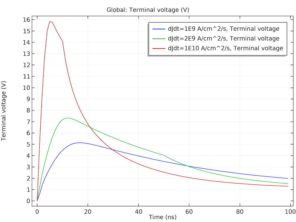
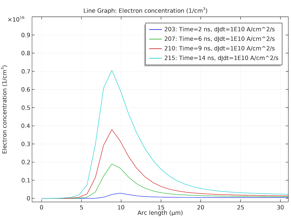
The left figure below shows the time evolution of the device voltage for the three current ramp rates. The right figure shows the electron concentration at a few selected time points for the current ramp rate of 1e10 A/cm2/s. They exhibit the typical behavior as expected from the initial accumulation of extra charge carriers in the drift region during the turn-on process. The figures compare well with Fig. 5.30 and 5.31 in Ref. 1.
Left: Initial voltage spike of the forward recovery. Right: Accumulation of electrons in the drift region.
The Reverse Recovery Model
The reverse recovery tutorial is approximately based on another device model that is found on page 256 of Ref. 1. In the reference, it is assumed that after the initial linear current ramp, the device suddenly becomes voltage-driven with a constant magnitude; however, this example uses the Electrical Circuit interface to model an inductive load with a flyback diode that contributes to the described current and voltage behavior.
The circuit contains two voltage sources in parallel, but only one is activated at a time in the study steps. One voltage source is for the on state and the other is for the switching process. A Global Equations node is added in the circuit interface to improve numerical stability for the case when the time derivative of a dependent variable is used in the definition of a variable, as shown in the screenshot below.
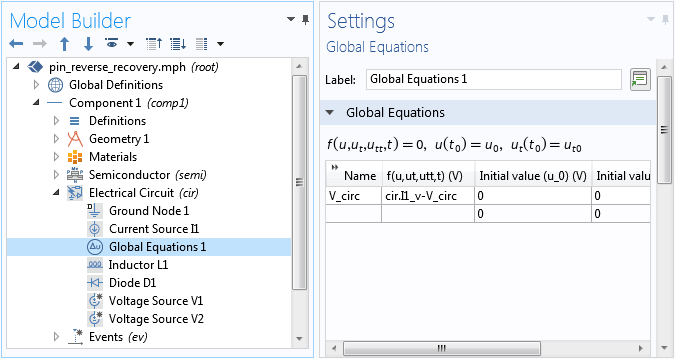
Using the Global Equations node in the Electrical Circuit interface improves numerical stability.
The Semiconductor interface simulates a diode of 80 um length and 1 mm2 cross-section area. Important effects, such as the Fletcher mobility model, Slotboom band gap narrowing, and Shockley-Read-Hall recombination, are included. Note that for the mobility model to take effect, the drop-down menus under the Mobility Model section in the Settings window for the Semiconductor Material Model node need to be set to the desired mobility model (Fletcher in this case); otherwise, the Fletcher Mobility Model subnode has no effect. See the screenshot below.
![]()
The mobility model has to be selected in the Semiconductor Material Model node in order for it to take effect.
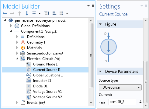
The bidirectional coupling between the electrical circuit and the semiconductor model is mediated by the Current Source node in the circuit. The current flowing into the electrical circuit is specified by the terminal current from the Semiconductor interface. The terminal voltage of the semiconductor metal contact is in turn specified by the voltage of the current source. See the screenshots below.
Settings for the bidirectional coupling between the circuit and the semiconductor model.
Similar to the forward recovery model, the Events interface is used to mark the abrupt changes in the slope of the applied voltage.
Setting Up the Time-Dependent Reverse Recovery Model
As mentioned above, choosing the correct initial condition is crucial for the time-dependent model to represent the actual physical system. In the case of reverse recovery, the initial condition should be given by the on state. Therefore, in the study setup, the time-dependent study step (Step 3) is preceded by a stationary study step that ramps the applied voltage from zero up to the steady-state voltage for the on state (Von), as shown in the screenshot below.
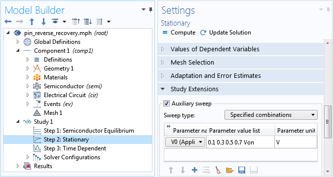
Using the Stationary study step to solve for the on-state solution as the correct initial condition for the time-dependent study step.
The Semiconductor Equilibrium study step provides a good initial condition for the Stationary step.
Similar to the forward recovery tutorial, the relative tolerance of the time-dependent step is set to 1e-5 for better accuracy. In addition, manual scaling of the dependent variables is used with values corresponding to the order of magnitude of each of the variables being solved for.
Reverse Recovery Result for a PIN Diode
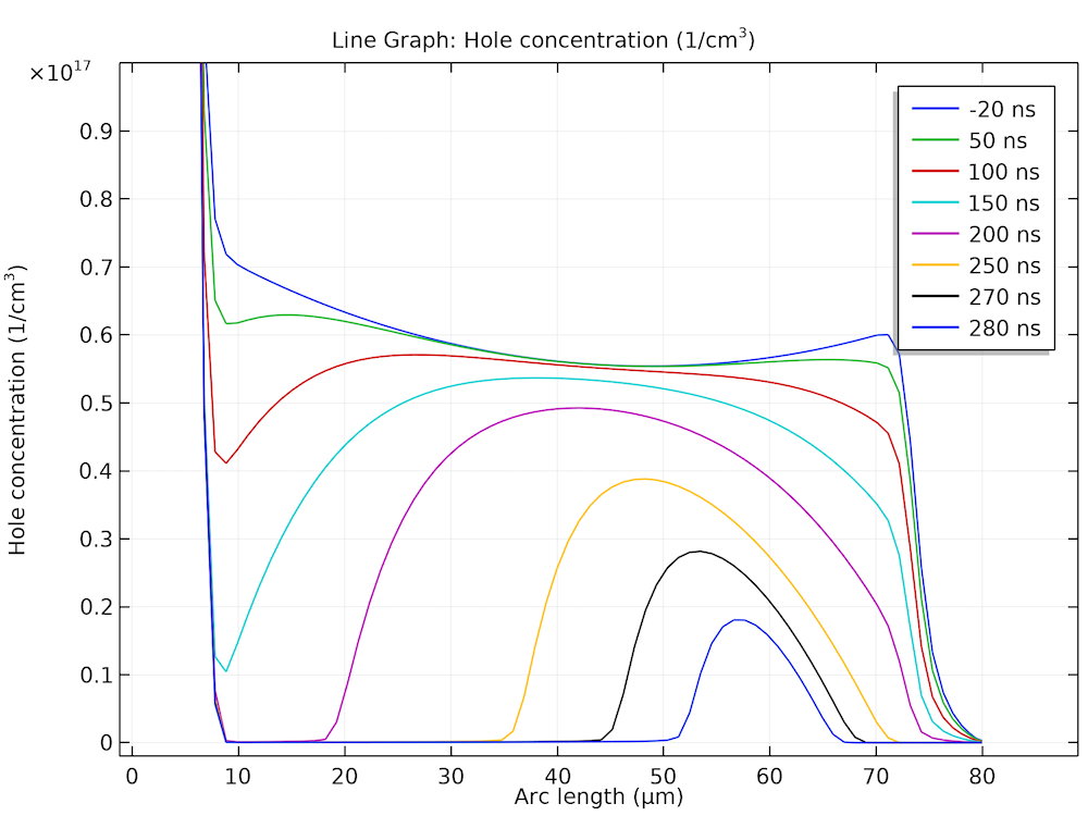
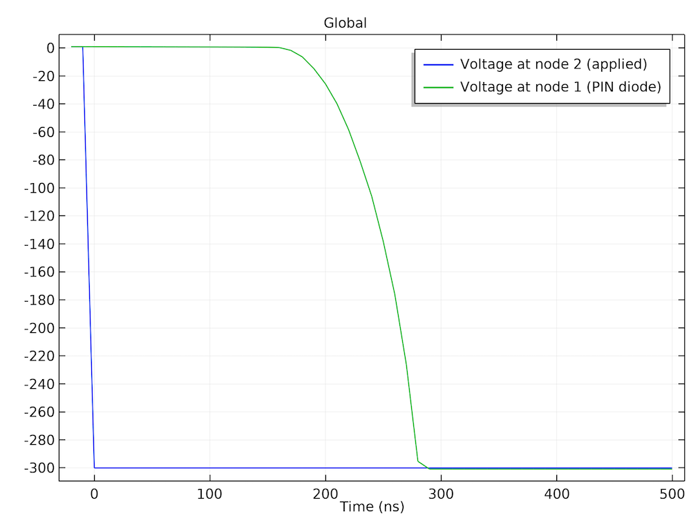
The figures below show the hole concentration profile at a few selected time points, the time evolution of the applied voltage and the device voltage, and the time evolution of the current. They are consistent with the behavior expected from the inductive load and the dissipation of the stored charge carriers in the drift region. The figures compare well with figures 5.42, 5.43, and 5.44 in Ref. 1.
Left: Dissipation of the holes stored in the drift region. Middle: The diode remains forward biased for a period of time after the applied voltage is switched, due to the stored carriers. Right: The current as a function of time after the switching.
Concluding Thoughts on Analyzing Carrier Dynamics in Semiconductors
In this blog post, we have highlighted the importance of selecting the appropriate initial conditions for time-dependent models to correctly describe the dynamical behavior of the physical system. We have also showed the use of the Events interface to mark abrupt changes in the time evolution as well as the bidirectional coupling of circuits to a semiconductor model. The use of a mobility model and a Global Equations node in the Electrical Circuit interface is also demonstrated. Please share with us how you apply these techniques in your simulations.
To try the forward and reverse recovery examples, click the links below:
You can also learn more about semiconductor simulation on the COMSOL Blog:
- Computing the Band Gap in Superlattices with the Schrödinger Equation
- Evaluating a Schottky Diode with a Semiconductor Benchmark Model
Reference
- B. Jayant Baliga, Fundamentals of Power Semiconductor Devices, Springer, 2008.





Comments (3)
Jose Santos
June 10, 2019Good morning Mr. Liu,
I am simulating an uniformly doped semiconductor material, and I need to apply a bias voltage or 30-40V through a metal contact. I need to simulate its time response. I could run simulations up to a bias voltage of 15V. However, I am getting errors as I increase the bias voltage. Do you have something in mind that could be causing this issue. I would really appreciate your response.
Respectfully,
Jose Santos.
Brianne Christopher
June 10, 2019 COMSOL EmployeeHello Jose,
Thank you for your comment.
For questions related to your modeling, please contact our Support team.
Online Support Center: https://www.comsol.com/support
Email: support@comsol.com
zahra maghduri
November 26, 2023Hello, how are you? I need help about simulating about Carrier Multiplication process in Comsol. Do you know about something about this subject?