
When you have solved a model, you want to visualize your results in the best way possible. Today, we will explain how to include geometry surfaces with your solution plots, by way of an RF modeling example.
About Our Demo Model
Substrate integrated waveguide (SIW) antennas are small devices that are showing promise for use in applications such as military and satellite communications. Very simple to implement, they make it easy to direct radiative waves. Visualizing results on these devices can give an integrated picture of the geometry, materials, and physical phenomena that are present. I asked my colleague, Jiyoun Munn, to teach me how to show RF radiation in an SIW antenna using the postprocessing tools available in COMSOL Multiphysics. Here’s what he told me.
Hide and Seek: Orienting Your Model
Below is the geometry of a model that we’ll use to explore some postprocessing techniques. We’ll include different surfaces for different geometric components in a solution plot. This kind of visualization is particularly helpful for guiding knowledge of the physics occurring in a device. It is also helpful for verifying that the hardware is operating correctly.
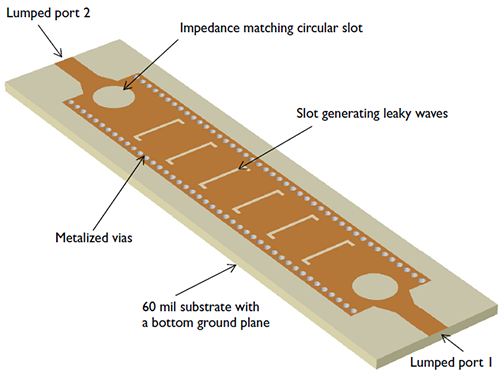
This antenna contains a copper microstrip overlaid on a dielectric surface (usually a mix of PTFE or Teflon and fiberglass) and a series of slots that are open to the environment. These each function as a radiation source, facilitating what are called “leaky waves”, or waves that escape from the waveguide through the slots. The slots are spaced so that waves exiting each slot will have a different magnitude, phase, and radiating energy. The lumped ports are the input (Lumped port 1) and output (Lumped port 2) where waves enter and leave the waveguide.
This model is named siw_leaky_wave_antenna.mph. The fully solved model is accessible from the COMSOL Model Libraries Update (under File > Help > Update COMSOL Model Library > Full Models > RF Module > Antennas). Upon opening the model, one of the first things you might notice is that the geometry contains several domains outside of the antenna itself. These are the air domain and perfectly matched layers (PML) that surround the model, but for visualizing purposes, we don’t want to see them. So the first thing we’ll do is hide these geometric entities.
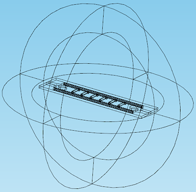
Right-click the View node under Component > Definitions and select Hide Geometric Entities. Make sure that the Geometric entity level is set to “Domain”. You can select a section of a domain by clicking on it (it will turn red when you move the mouse over it):
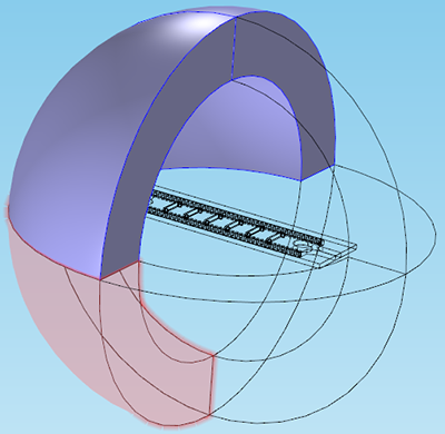
Once you’ve hidden each section, right-click the View node and choose Hide Geometric Entities again. This time, select all of the circular domains that surround the antenna. This leaves us free to see the hardware clearly.
Note: This same feature also enables visualization of the interior of the modeling domain. While we don’t need to see the inside of the hardware for this model, this capability can give a good look into the physics happening inside a device. We’ll demonstrate this feature in Part 2. Stay tuned!
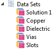
Now, expand the Data Sets node under Results. Duplicate Solution 1 four times by right-clicking its node and choosing Duplicate. We’ll set each of the new solutions to correspond to one part of the geometry, so that we can plot different results on different areas of the hardware. Rename each new solution (preserve Solution 1 as it is) according to the part of the geometry it will correspond to — Copper, Dielectric, Vias, and Slots.
For each of these solutions, we’ll need to select the appropriate geometric entities. Right-click the Copper solution and choose Add Selection. From the Geometric entity level, choose Boundary. Then click on the microstrip. Since we will only be looking at the top of the antenna, there is no need to select the copper areas on the bottom.
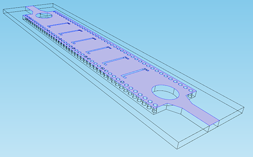
Do the same for the dielectric, vias, and slots (see the images below to check your selections).
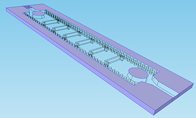
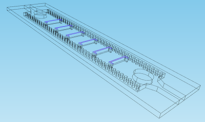
To select the vias, there are a couple of methods that are easier than selecting each section of each cylindrical boundary one by one. If the vias have been previously organized into a group, you can choose that group as the data set. If they haven’t, the simplest way to select all of the boundaries is to arrange the graphics view so that all the vias are in vertical columns and you can draw a selection box around each set. Click and drag the mouse until you’re happy with the model orientation.
The Select Box tool is located in the toolbar at the top of the graphics window (![]() ). Click and drag the box carefully around the elements you want to highlight (each column of vias, in this case):
). Click and drag the box carefully around the elements you want to highlight (each column of vias, in this case):
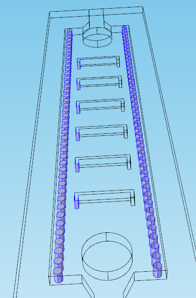
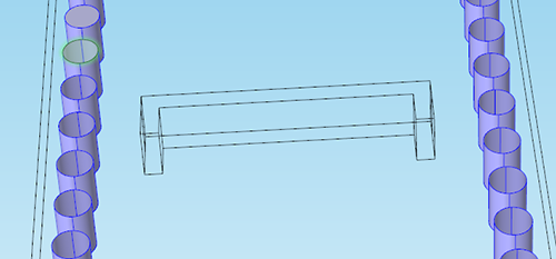
You may end up with a few more boundaries selected than you want (as in the figure above, where several boundaries on the slots are highlighted in purple). To deselect these, click on each one.
Click on the circular boundary at the top of each via hole in order to deselect it. This is easier if you zoom in. Since the vias are open to the environment on top and in the center, we don’t want the top boundary to look like metal. (This might seem like a long process, but it’s faster than selecting each boundary of each cylinder one by one!)
Dressing Up Your Look with Material Colors, Deformations, and Radiation Patterns
Now that we have each data set, we can begin adding results plots. Right-click the Results node and add a 3D plot group. I prefer to not see data set edges in this surface, so I have unchecked the Plot data set edges box in the plot settings window.
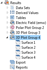
Right-click the new plot group (3D Plot Group 4) and choose Surface. Since we’re plotting on several different components — copper, dielectric, metal vias, slots — we’ll need several surfaces. Duplicate the surface you just created three times. Your results node should now look like the one below.
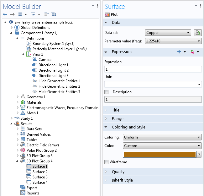
First, let’s make the microstrip a nice copper color. Go to Surface 1. In the settings window, change the data set to “Copper”.
To save some computational resources, we’ll set the expression to a dummy variable. Since we’re not plotting results on this part of the geometry, there’s no need for a physics expression. Instead, set the expression to 1.
Go to the Coloring and Style tab and change your settings to match roughly what’s shown below. Make sure to set the Coloring selection to “Uniform” and then choose a custom color that’s close to copper.
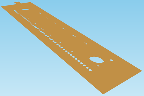
Initially, it’s going to look a little weird. But that’s okay; once we add colors for the other materials, the geometry will start to become clearer.
Next, let’s add color for the dielectric and the vias. We’ll do this exactly the way we did for the copper microstrip (choosing colors that match the materials). For the dielectric (if you recall, this is usually made of a PTFE laminate), choose an off-white color. For the vias, choose a metallic silver.
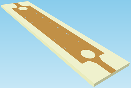
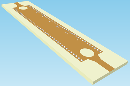
Our geometry is starting to look a little more realistic. For the slots, though, we’ll plot results from the simulation data. The slots are where the leaky waves are generated, so we’ll want to show how strong the electric field is in each one, and how it changes from one end of the waveguide to the other.
For Surface 4, set the Data set to Slots. This time, choose Replace Expression in the Expression tab. Navigate to Electromagnetic Waves, Frequency Domain > Electric and double-click Electric field norm (emw.normE). Click Plot:
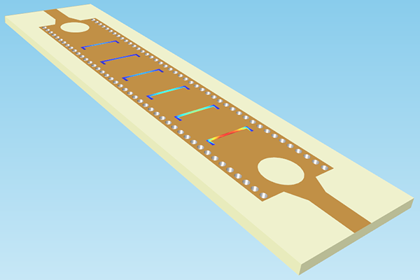
We can see from the results we just plotted that the electric field is highest near the input port and weakens toward the output port. But we can’t tell much else, since the plot is so small. Let’s see if we can get a better view of the radiation pattern.
Right-click 3D Plot Group 4 and choose More Plots > Far Field. A far-field calculation behaves as if the antenna is very far away and so gives a wide view that shows both the direction and the intensity of the radiating energy. As with the surface plot we created in the slots, we want to know how strong the electric field is and how it changes.
Go to Replace Expression > Far field and double-click Far-field norm (emw.normEfar). Click Plot.
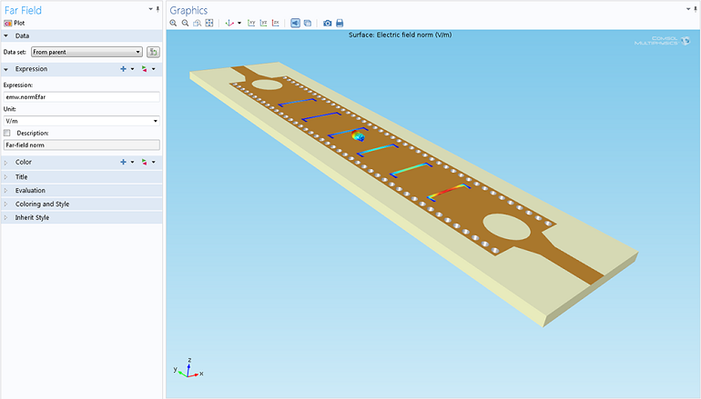
We can see the 3D radiation pattern in the center of the microstrip, but it’s very small. Since we are treating the waveguide as though it is very far away, we can’t really tell what’s going on from here. In order to see it more clearly, we’ll magnify it.
This is easy to do; multiply the expression by a factor of 10. You can do this by adding 10* in the expression in the field, so that the whole expression becomes 10*emw.normEfar. Click Plot again.
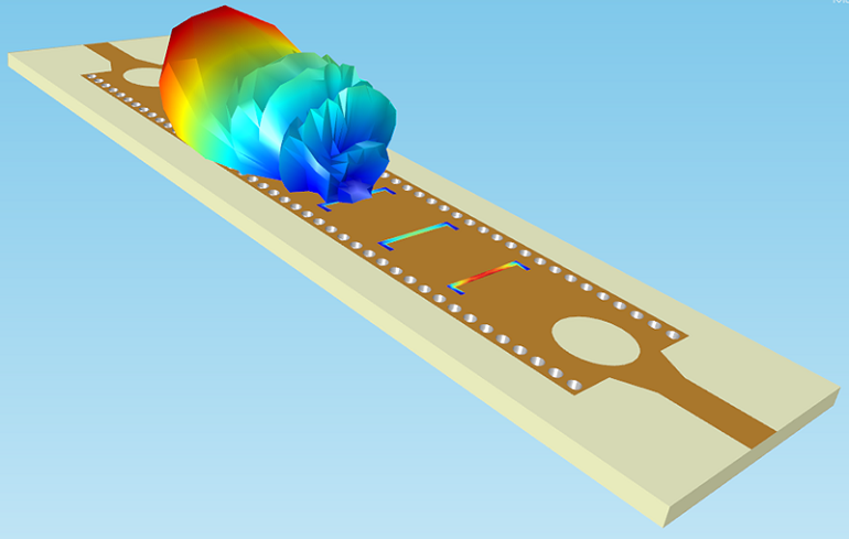
It’s now obvious that we need to refine the resolution a bit, but we’ll save this for last. We can see the 3D pattern of the radiating energy now.
Tilt the antenna by clicking on the model and dragging the mouse. With a certain orientation, you’ll be able to see the far-field radiation pattern extending below the substrate:
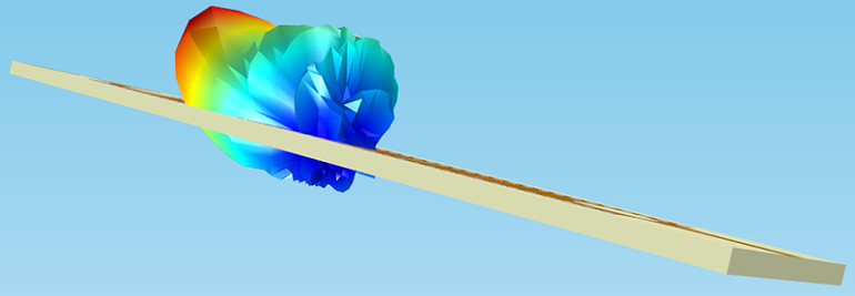
For visualization purposes, we may want to see the entire pattern more easily from the top, rather than needing to look at the waveguide from the side, where we can’t see the slots. Let’s shift the antenna geometry down a little bit, so that the entire far-field plot is visible on top of it.
To do this, right-click Surface 1 and choose Deformation. We’re adding a very simple deformation, a translation in the z-direction only. In the Expression section, set the x-component to 0, the y-component to 0, and the z-component to -5. Check the Scale factor box, and set it equal to 1.
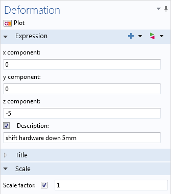
Click Plot. Our geometry now looks pretty funny, because we’ve shifted one part of it down by 5 millimeters, but the rest has stayed put:
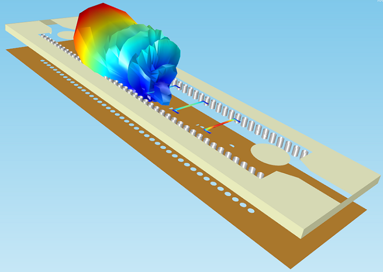
We don’t have to redo this step for each surface, though. We can copy the deformation and paste it into the other surface plots. Right-click Deformation 1 and choose Copy. Then right-click each of the other surfaces (2-4) and choose Paste Deformation. Now, the far-field pattern should be sitting right on top of the antenna.
Smoothing out the Ridges: Refinement
Almost perfect! Finally, let’s refine the far-field visualization. Click on the Far Field 1 node and expand the Evaluation tab. Here, you’ll see options for two different angle resolutions: \theta and \varphi. By default, they are set to \theta = 10 and \varphi = 20. These angles represent the number of rotational samples that the simulation will check for, elevation and azimuth; the higher the angle number, the smoother and more accurate the pattern visualization will be.
Try setting them both to a higher sample number, for example, 45. This will give a higher resolution, but still not as smooth as we might like. For a very smooth visualization of the 3D radiation pattern (though also somewhat heavy computationally), set them both to 180. Click Plot again. Now we have a clear picture of the electric field strength and direction:
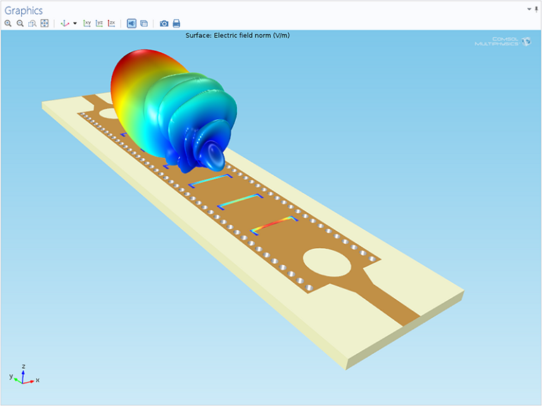
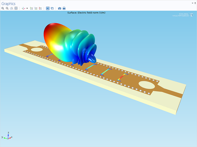
Congratulations! You’ve completed a complex visualization of the antenna and the electric field caused by the wave radiation, complete with surfaces on individual geometry selections, realistic material colors, and deformations. Try tilting the model in the Graphics window to see which view you like best.
Visualizing tools like the ones we used in this model are often very helpful for understanding the physics phenomena in a device, sharing your simulation results with others, and generating clean and beautiful results plots. I hope you’ve enjoyed learning how to plot these solutions and that you’ll be able to apply these techniques to other models in the future.
Further Reading
- Download the SIW Leaky Wave Antenna model
- Read more about postprocessing techniques


Comments (0)