
When simulating electromagnetic devices, a common mistake is putting everything into a model at the same time, including a complicated geometry, complex material properties, and a mixed bag of boundary conditions. This makes the model run for a long time and you might get frustrated when your simulation results are physically wrong, without any clues as to why. Today, we will discuss how to efficiently set up simple RF, microwave, and millimeter-wave circuit models in the COMSOL Multiphysics® software.
How to Set Up RF, Microwave, and Millimeter-Wave Circuits in COMSOL Multiphysics®
Regardless of the characteristics of your device, whether it is resonating, radiating, or attenuating, the rule of thumb for your electromagnetics simulation is simple: You need to make the modeling process efficient, as discussed in a previous blog post. Even if you are confident in your design, it is better to start with a simple structure so you can ensure that the modeling process is correct for the given basic geometry before adding complex design elements.
When electromagnetic waves are not radiating but captured in a device, they are guided, confined, or attenuated through a structure. The physical phenomena inside passive microwave and millimeter-wave circuits can be addressed via electromagnetic (EM) simulation by solving Maxwell’s equations.
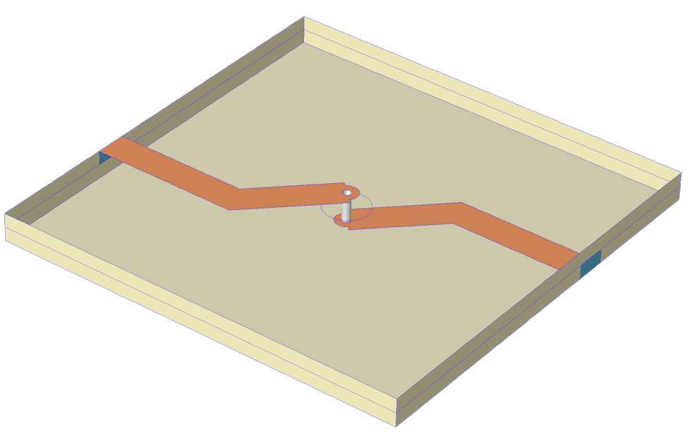
An electromagnetic wave confined via a microstrip meander line connected to SMA receptacles.
To efficiently describe the passive circuit measurement in a real lab environment, it is necessary to pick the right physics features and boundary conditions. It is challenging to accurately reflect real-world conditions in a model, while also being both time and memory efficient.
Below, we summarize some real-world measurement and testing situations and the possible modeling features to choose in COMSOL Multiphysics:
| Real World | Simulation Environment | |
|---|---|---|
| Basic | Advanced | |
| Metal trace, ground plane, and conductive enclosure | Perfect electric conductor |
|
| Open space | Scattering boundary condition | Perfectly matched layer |
| Network analyzer measuring S-parameters for input matching and insertion loss properties | Port or lumped port | Numeric TEM port |
| Surface mount devices such as resistors, inductors, and capacitors | Lumped element: R, L, and C | Lumped element: series or parallel LC and RLC |
| Complicated device measurement data | Two-port network: S-parameter | Two-port network: Touchstone import |
When setting up a passive circuit model, you don’t need to have a lot of complicated boundary conditions in the beginning of your modeling process. You can build a circuit, especially for low frequencies, using just two features in COMSOL Multiphysics and the RF Module. Let’s go over this process using a microstrip line example.
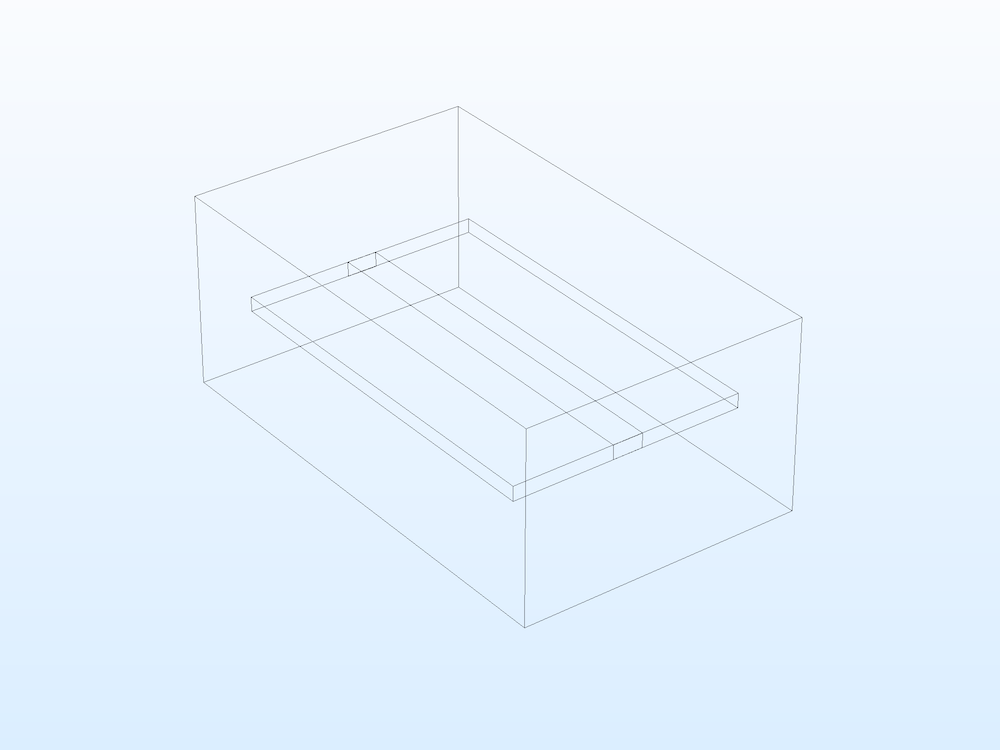
The geometry of a microstrip line.
A microstrip line circuit is composed of five objects, each with a specific purpose:
- Block that acts as a metallic enclosure filled with air
- Block that acts as a substrate
- Rectangle that acts as a printed metallic trace
- Rectangle that acts as lumped port 1 for excitation
- Rectangle that acts as lumped port 2 for termination
The materials include a dielectric substrate (user defined) and air, which encloses the entire domain.
You must then choose the correct physics features for the model:
- Perfect Electric Conductor boundary condition, which mimics metallic surfaces with a high conductivity
- Lumped Port boundary condition, which excites or terminates the circuit and measures S-parameters
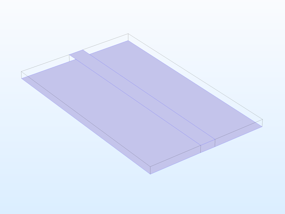
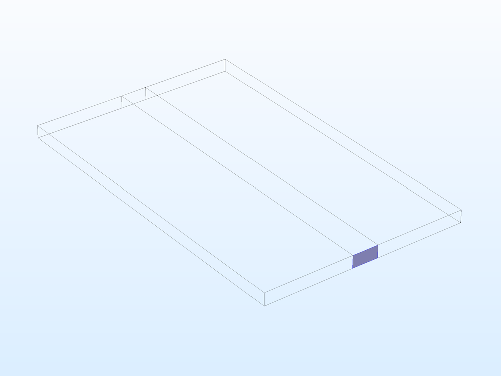
The metallic part in the microstrip line circuit: top copper trace and ground plane (left) and a Lumped Port boundary condition at one end of the microstrip line (right).
The simulation may only take a few seconds to solve at the intended operating frequency. You will get the default S-parameter evaluation and electric field distribution plot for a single frequency. When the simulation is performed on multiple frequencies, the electric field distribution plot, S-parameter plot, and Smith plot are plotted by default. You can also evaluate port impedance as necessary.
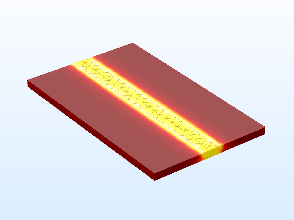
The electric field distribution on the surface of the substrate is visualized with the mesh view of the microstrip line.
The RF Module lets you add other physical effects to your electromagnetics simulations. This means that you can study all of the physical phenomena and define the properties to suit your unique needs. When validating your device design, it is useful to take into account not only a single physical effect, but also multiple physics — and to know the underlying physics involved.
Find more information on how to capture the details of underlying physics in previous blog posts on modeling metallic objects in wave electromagnetics problems and using perfectly matched layers and scattering boundary conditions for wave electromagnetics problems.
Next, you can start to design your microwave and millimeter-wave circuit, whether it is a coupler, power divider, filter, or wideband device.
Developing Microwave and Millimeter-Wave Circuits with the RF Module
The Application Library for the RF Module offers RF, microwave, and millimeter-wave examples for a wide range of applications. The tutorial models include conventional devices, such as basic transmission lines, couplers, power dividers, filters, and coils, as well as multiphysics examples like microwave ovens, SAR calculation, tunable filters, and more. There is also a circulator example that uses ferrite material properties.
Traditional Filter, Coupler, and Power Divider Examples
Couplers, power dividers, and filters are fundamental devices in microwave engineering. They are good introductory examples for learning how to model microwave circuits in the COMSOL® software. It’s also relatively easy to validate your simulation results with well-known textbook examples.
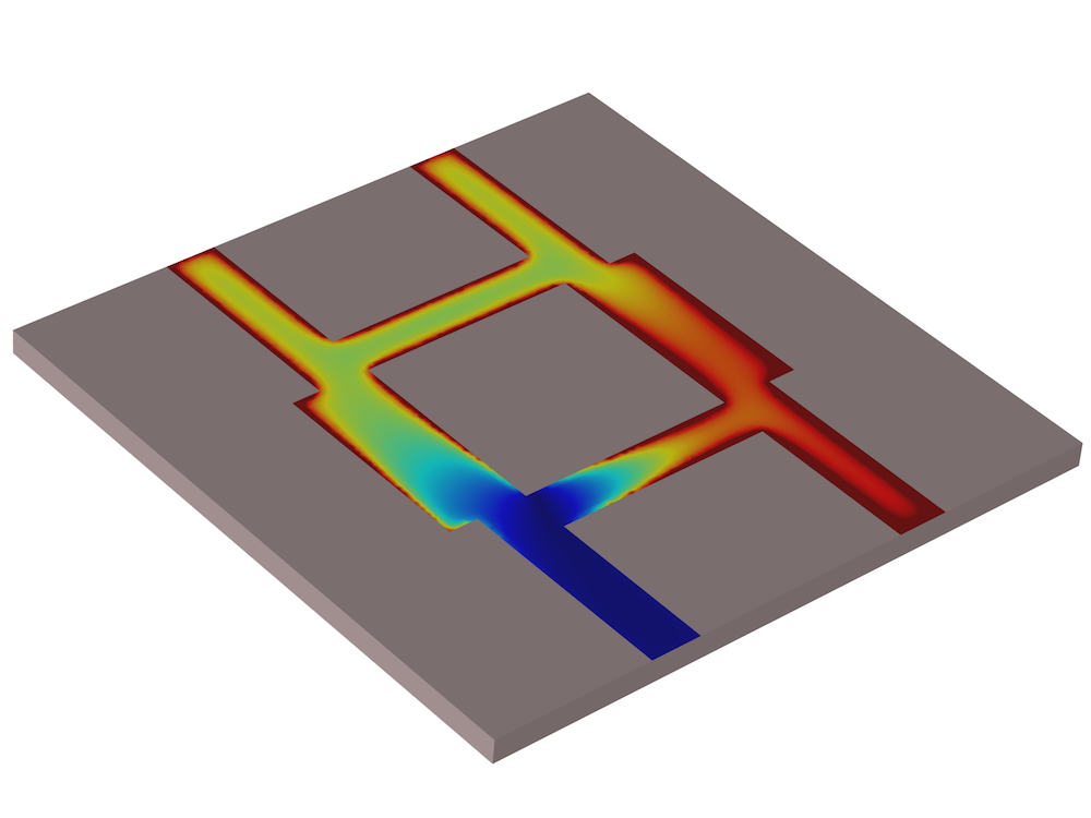
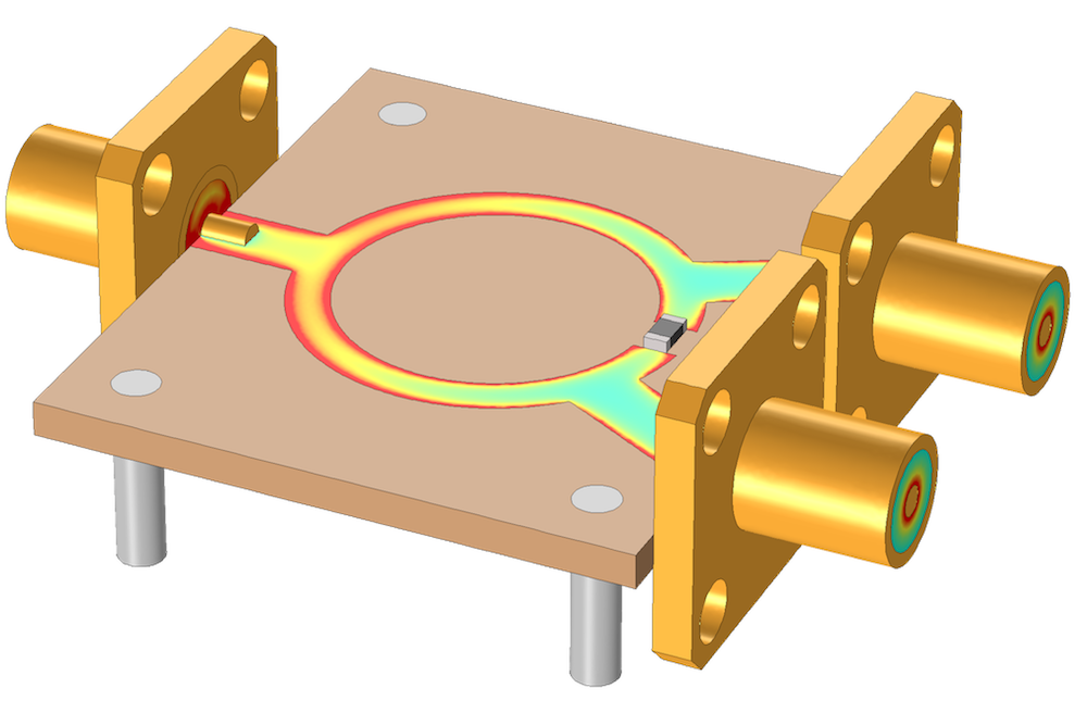
Textbook examples of a branch line coupler, quadrature 90° hybrid (left) and Wilkinson power divider (right).
Filters are essential in microwave circuits to refine signals in RF and microwave systems.
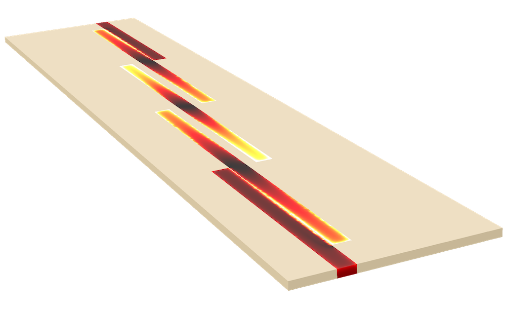
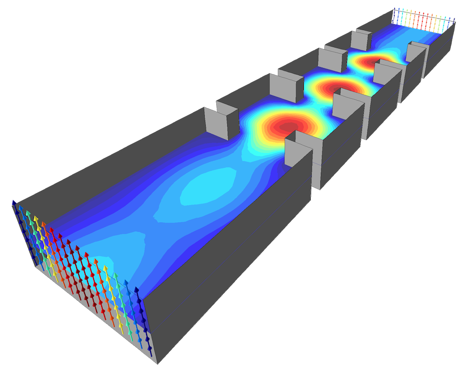
A coupled line filter (left) and waveguide iris filter (right).
Passive devices are not limited to the conventional shape of circuits on PCBs. For instance, another device is made up of periodic structures that can provide a frequency response for a bandpass or bandstop, called a frequency-selective surface, split ring resonator. In the example below, the signals around the center frequency are the only ones that are able to pass through the layer of the periodic complementary split ring resonator.
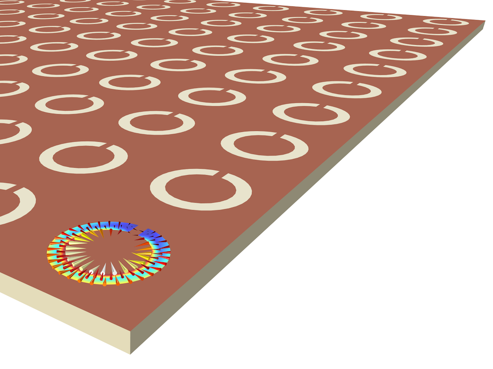
A model of a frequency-selective surface, complementary split ring resonator. You can use periodic boundary conditions to model an infinite 2D array on one unit cell.
Adding More Physical Effects for Multiphysics Simulation
Due to heat expansion, external force, or the behavior of piezo materials, the structure of a circuit can be distorted. The surface can be warped nonuniformly, which can cause nonuniform reactance distribution that cannot be simply addressed via a geometric parametric sweep. By including the real-world physical effects in your design, you can accurately analyze complex devices, such as tunable filters controlled by piezoactuators, and realize true multiphysics simulations.
Animated multiphysics examples of a tunable cavity filter controlled by a piezoactuator (top) and a printed low-pass filter affected by external force (bottom).
To perform multiphysics simulations, you just need to combine other physics with your microwave circuits, such as heat transfer to simulate microwave heating or structural mechanics to see how structural deformation affects the electromagnetic behavior of your device. Though you are handling multiple physics, you are still working in the same environment and using the same workflow.
Accelerating EM Simulation Using Reduced-Order Modeling Techniques
Certain EM devices, such as bandpass-filter-type high-Q devices in the frequency domain, are computationally expensive to simulate. The RF Module offers two analysis types to help accelerate bandpass filter modeling: asymptotic waveform evaluation (AWE) and frequency-domain modal analysis.
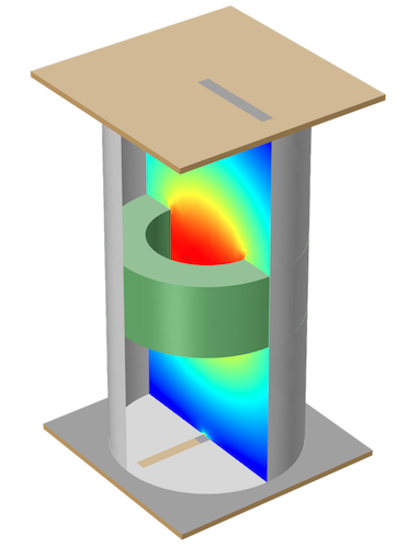
The Evanescent Mode Cylindrical Cavity Filter tutorial model shows the usage of the AWE method. It is very useful when simulating a single resonant circuit with many frequency points.
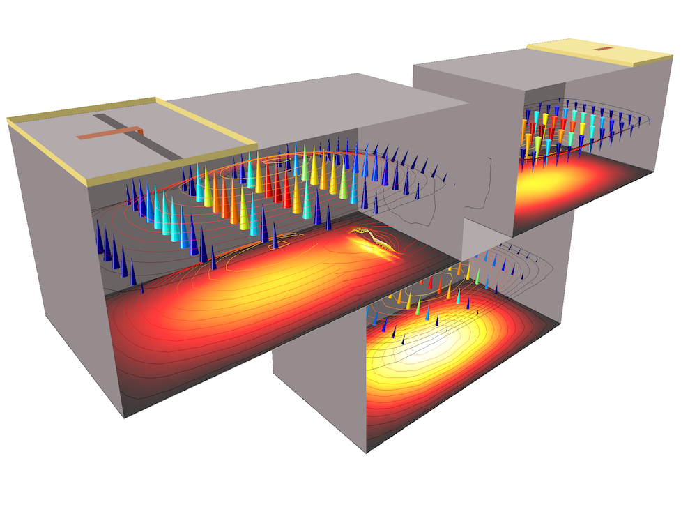
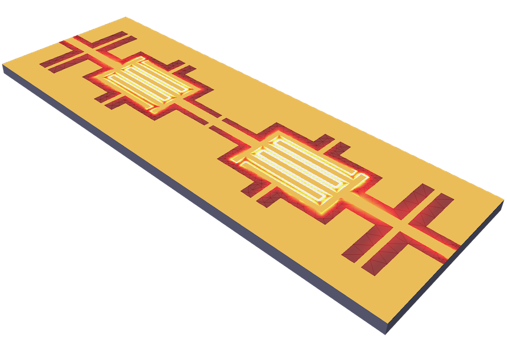
These cascaded rectangular cavity filter (left) and CPW bandpass filter (right) examples in the Application Libraries present the advantage of using the frequency-domain modal method when analyzing bandpass-frequency responses of a passive circuit resulting from a combination of multiple resonances. Here, eigenfrequency analysis is key to capturing the resonance frequencies of an arbitrary shape of a device.
Through the AWE or frequency-domain modal method, you can get a very fine frequency response, which could result in a huge file that contains a tremendous size of data. Usually, designers are only interested in S-parameters for passive microwave circuits, so it is not required to save all of the data in the entire simulation domain, but only data associated with the boundaries for S-parameter calculation: lumped port and port boundaries. These boundary sizes are relatively small and the file size of a model running the model order reduction techniques can be reduced a lot by storing the solution only on relevant port boundaries.
Time-Domain Reflectometry in Circuits
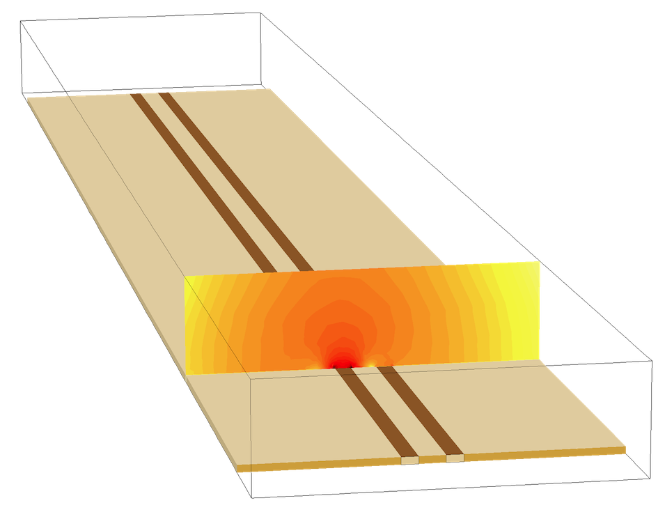
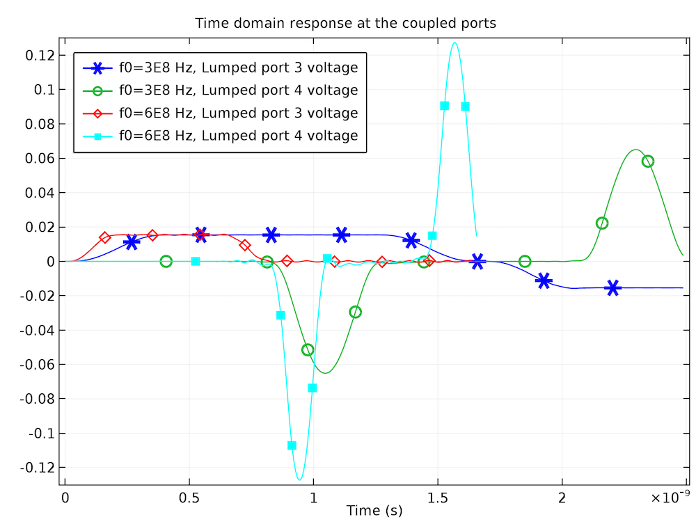
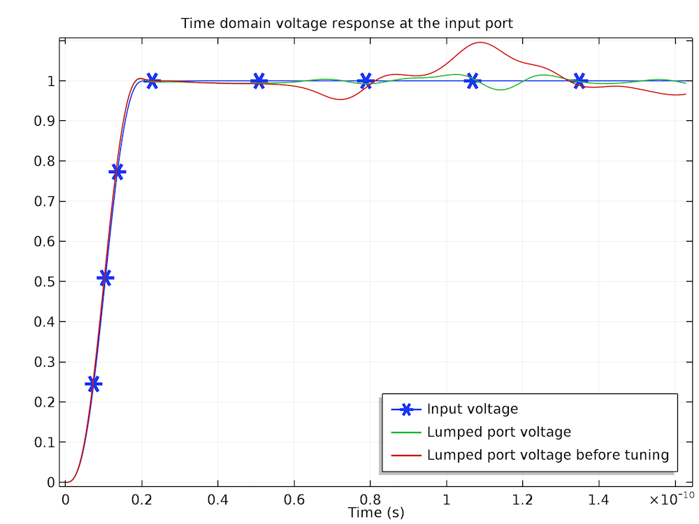
The Electromagnetic Waves, Transient physics interface simulates electromagnetic wave propagation in the time domain, where the time-domain reflectometry (TDR) of a microwave circuit can be calculated. By performing a TDR analysis of your device, you can predict the quality of a signal transmitted through the circuit. The voltage distortion due to the coupling between transmission lines and the impedance mismatch from any discontinuity on a transmission line degrades the quality of a signal: essence of signal integrity (SI). Since there are more demands for high-speed interconnect devices handling a higher data rate in the market, there is a fast-growing interest in the signal integrity application area. The examples below illustrate the TDR for two cases: the unwanted coupling between two adjacent microstrip lines and the impedance mismatch from a metalized via, respectively. In both cases, the unwanted effects are manifested in the time evolution of the lumped port voltages.
A microstrip line crosstalk model (left) and its TDR at each port, showing that the higher data rate signal causes the stronger crosstalk on another signal path (right).
TDR analysis can be used to optimize impedance matching properties for the design of high-speed interconnects.
Rapid Prototyping and Analyzing Transmission Line Equations
Interest in the millimeter-wave frequency range is growing due to upcoming 5G mobile network applications that need to support higher data rate communication. Computationally cost-effective simulation helps quickly validate the concept of a prototype. When a waveguide is operating on its dominant mode, 2D modeling techniques help to reduce the simulation time drastically.
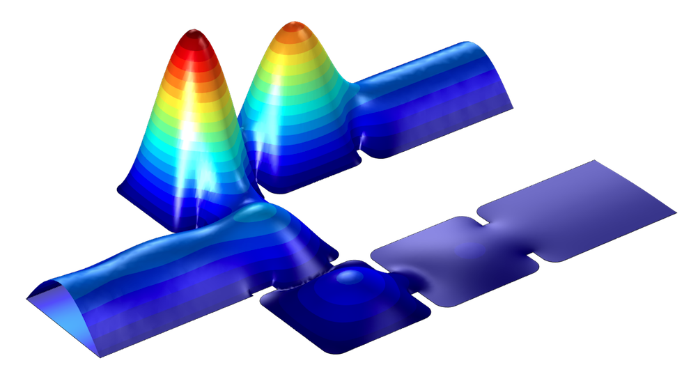
A diplexer is a device that combines or splits signals into two different frequency bands, widely used in mobile communication systems. This waveguide diplexer example simulates splitting properties using a simplified 2D geometry.
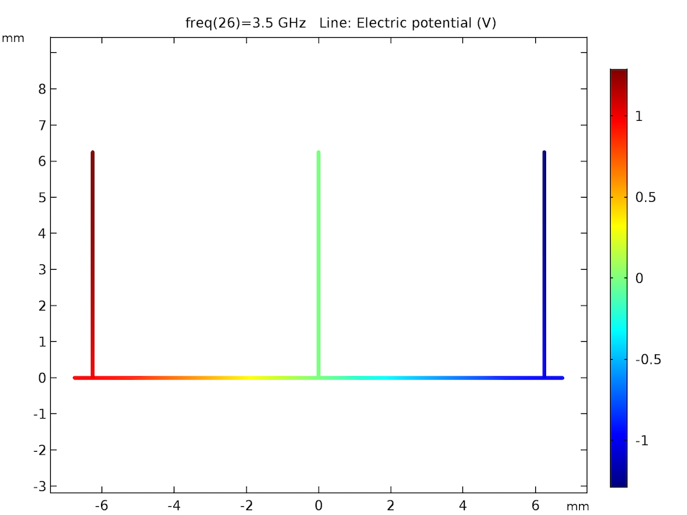
When the coupling between transmission lines is marginal, the Transmission Line physics interface will save time and resources, too. A simulation that usually takes several minutes to hours can solve in a few seconds with transmission line equations.
A traditional low-pass filter (left) and 4×4 Butler matrix (right).
Once the basic performance of a transmission line circuit is evaluated, the design can be extended to connect to a 3D model.
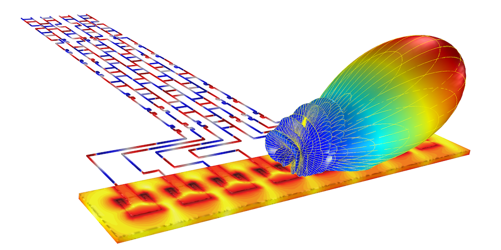
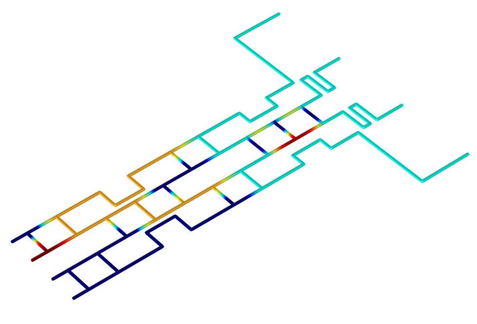
An 8×1 phased array antenna using an 8×8 Butler matrix at 30 GHz: a combination of fast transmission line analysis and 3D full-wave FEM simulation.
Final Thoughts on Modeling Microwave Circuits
Here, we have discussed different techniques for modeling microwave circuits, as well as examples of devices that can be designed with RF simulation. With this information and the featured examples, you can design passive circuits in COMSOL Multiphysics, while maintaining optimized computational efficiency.




Comments (1)
Michael Haile
December 17, 2018how can design An 8×1 phased array antenna using an 8×8 Butler matrix at 30 GHz: a combination of fast transmission line analysis and 3D full-wave FEM simulation??
can you send me by makehaile3@gmail.com