
Bright light-emitting diodes (LEDs) are revolutionizing the lighting industry and blue LEDs in particular are ushering in a new age of widespread efficient LED lighting. The importance of blue LEDs was marked by this year’s Nobel Prize in physics, which went to the inventors. But, because bright LEDs are driven by larger currents, they suffer from reduced efficiency — a phenomenon known as LED droop. Using multiphysics simulations, we can investigate and understand the mechanisms behind LED efficiency.
Efficient Bright White LEDs
Light-emitting diodes (LEDs) are incredibly efficient compared to traditional lighting technology. LEDs typically require just 10 to 20% of the power needed to run an equivalent incandescent bulb and have operational lifetimes that are over 25 times longer.
LEDs vs. Traditional Light Bulbs
LEDs achieve their drastically improved performance by functioning in a very different way than traditional wire-filament bulbs. LEDs are semiconductor devices that emit light when electrons in the conduction band transition across the bandgap via radiative recombination with holes in the valence band. Under normal operation, this process produces very little heat and this allows a large proportion of the driving energy to be converted into light.
Incandescent bulbs rely on resistive heating of a filament, which emits light when it becomes hot enough to glow. This uses a lot of energy just to heat the filament and only a small fraction of output energy goes into light production. The high temperature involved also leads to shorter lifetimes, as burnt out filaments are nearly always the cause of incandescent bulb failures.
Why Color Matters for LEDs
Unlike incandescent bulbs, LEDs emit light over a very narrow range of wavelengths, leading to complaints about the “unnatural” quality of the light produced by early LED bulbs.
Red, green, and yellow LEDs have been around for decades, but it is the invention of the blue LED that has enabled bright white efficient LED lighting to become a reality. Blue LEDs greatly improve the brightness and spectral quality of LED emission. What difference does the color make?
Well, blue LEDs are so crucial because blue photons are towards the upper end of the energy range that is detectable by human eyes. This allows blue photons to be used to stimulate broader emission from phosphor layers around the LED casing, resulting in emission of a range of lower energy photons. This in turn creates a broader emission spectrum, which people often describe as “warmer”.
Alternately, blue LEDs can be combined with red and green LEDs and their relative brightness can be balanced to create any desired hue. This opens up the prospect of customizable lights where both the brightness and color can be varied. Indeed, that idea has sparked a revolution in the lighting industry. The race is on to develop new efficient and customizable lighting products.
Modeling Blue LEDs with Multiphysics Simulation
Although LEDs offer a huge improvement in efficiency over previous lighting technology, there are still some science and engineering challenges to overcome.
Unwanted Effect: LED Droop
In particular, the efficiency of LEDs decreases with increased driving current density, leading to LED droop. This means that in order to maintain efficient light production, LEDs must operate at very low currents. Due to LED droop effects, we must either increase the area of the LED device or add more LEDs to a bulb in order to increase brightness without compromising efficiency.
If we can eliminate LED droop, LEDs could be made much brighter simply by driving them with larger currents. That would then also reduce the financial expense and environmental impact of manufacturing LED bulbs. The cause of LED droop is the subject of much ongoing research. One way to gain some insight into the problem is to use multiphysics simulations to investigate possible mechanisms that might be responsible for the effect.
Multiphysics Simulation Example
As an example, consider the first high-efficiency blue LED for which the 2014 Nobel Prize in Physics was awarded.
The large bandgap required for blue photon emission is achieved using gallium nitride based materials. Specifically, an InGaN/AlGaN double heterostructure device was used in which a layer of the lower bandgap InGaN material is sandwiched by larger bandgap AlGaN. The device is doped to form a p-i-n diode, with the light-emitting InGaN layer at the center of the intrinsic region.
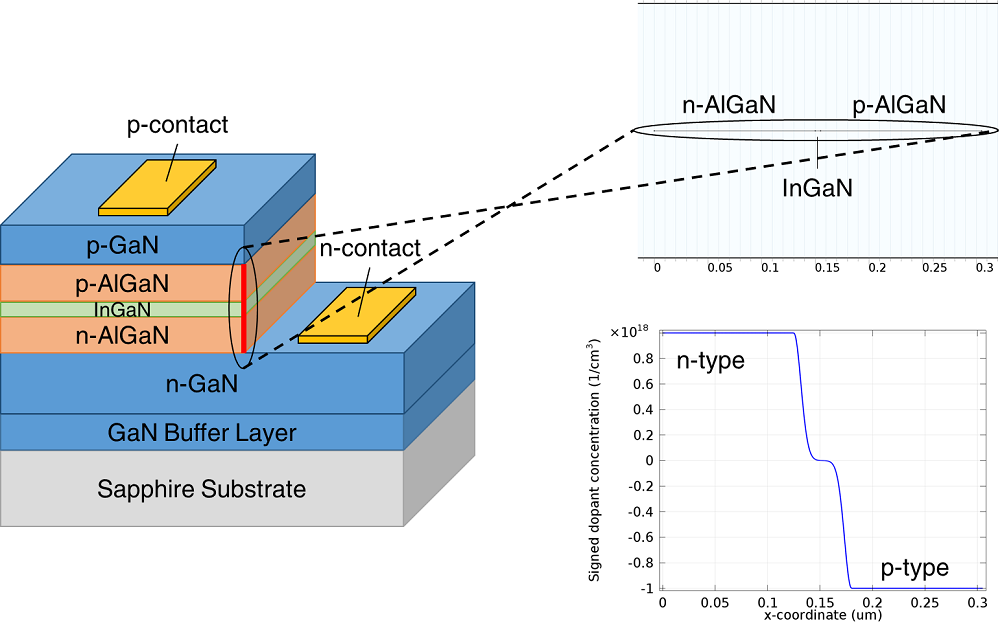
Geometry and doping of a blue LED device. Left: Representation of the layered structure of the device. A trench is etched into the n-doped layer to allow an n-contact to be placed and a p-contact is deposited on the surface. Top right: The model geometry is a 1D cross section through the active double heterostructure section of the device. Bottom right: The signed dopant concentration throughout the device shows that the light-emitting InGaN layer is in the intrinsic region of the p-i-n diode structure.
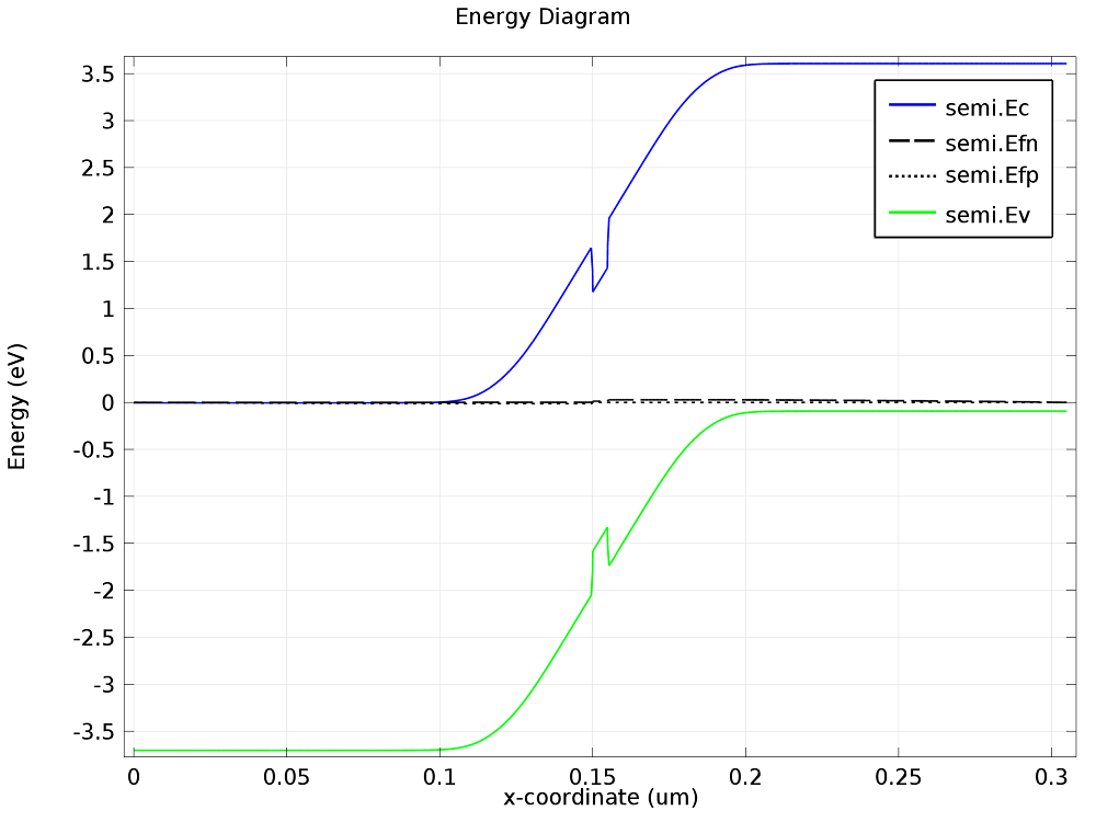
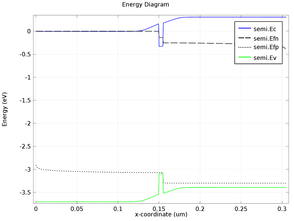
The double heterostucture design helps to maximize the efficiency of the LED device. The lower bandgap InGaN layer forms a potential well, which captures electrons in the conduction band and holes in the valence band. At equilibrium, when no voltage is applied, the built-in potential across the p-i-n junction causes a potential barrier that prevents current from flowing. Application of a forward bias reduces the height of the barrier and allows carriers to occupy the potential well in the InGaN layer.
This can be seen by plotting the energy diagram for the device at two different applied voltages, as shown below:
Energy level diagrams for the double heterostructure LED. Left: Zero bias. Right: Forward bias. The InGaN layer, which spans 0.15 ≤ x ≤ 0.155 μm, creates a potential well in both the conduction and valence bands. The potential barrier between the n-type and p-type sides of the device is reduced by the application of the forward bias. The conduction and valence bands are labeled semi.Ec and semi.Ev, respectively, and the electron and hole quasi-Fermi levels are labeled semi.Efn and semi.Efp.
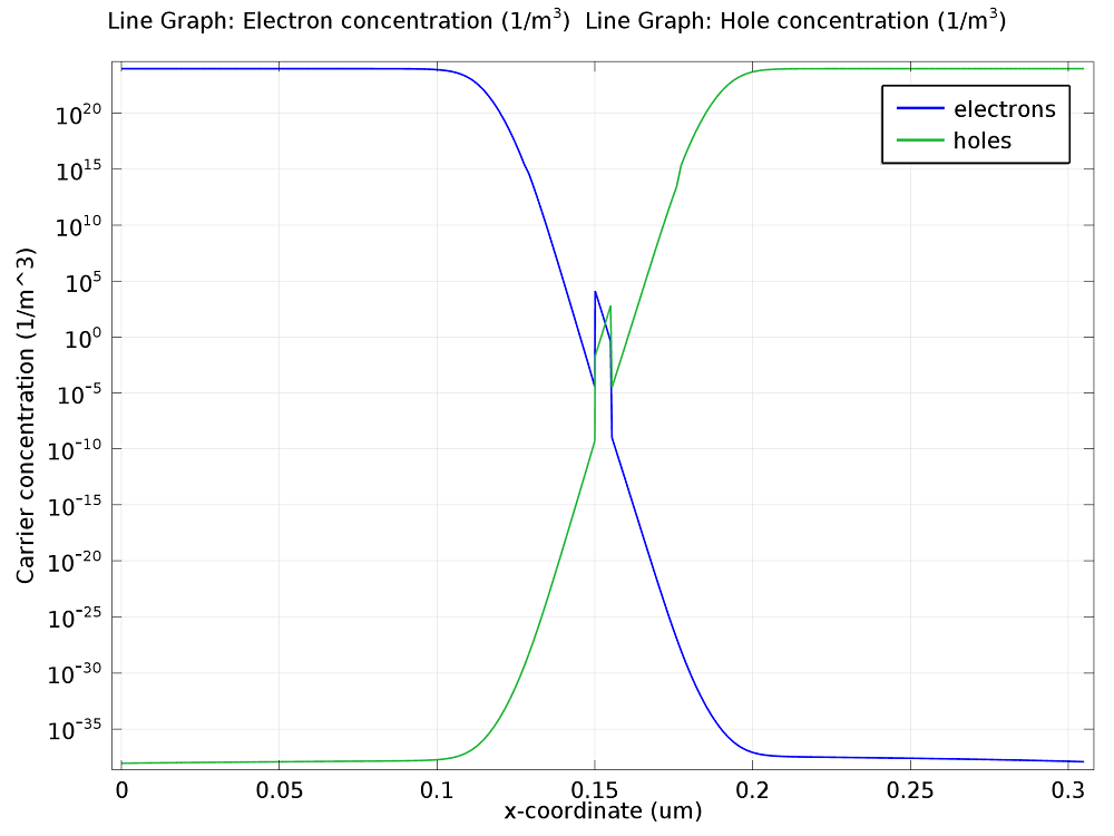
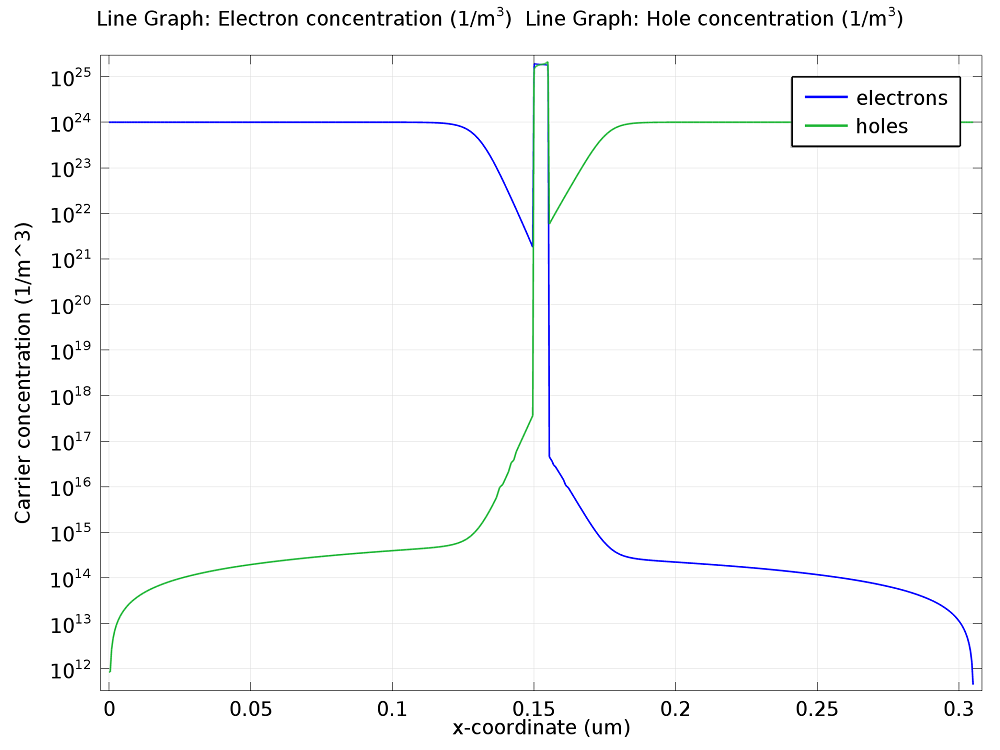
Along with reducing the potential barrier across the device, applying a forward bias also affects the quasi-Fermi levels. This has important consequences for the carrier density throughout the device. At zero bias, the quasi-Fermi levels are far from the band edges, resulting in a low carrier population within the InGaN potential well. When a forward bias is applied, the quasi-Fermi levels overlap the conduction and valence bands in the potential well, resulting in a high concentration of both electrons and holes in the InGaN layer. These effects can be seen in the next two plots showing carrier concentration.
In order to recombine, an electron and hole both need to be at the same x-coordinate, so the potential well localizes the emission to within the InGaN layer. As the desired wavelength is emitted only by the InGaN material and the localization of the emission increases the proportion of recombination occurring within the InGaN layer, the efficiency of the LED increases.
Carrier concentrations throughout the device. Left: Zero bias. Right: Forward bias. In both of the above cases, the InGaN potential well catches electrons and holes. However, the carrier densities in the potential well are drastically increased by the application of a forward bias.
The emission spectrum from the InGaN material can be calculated from the carrier dynamics in this region using a parabolic band approximation and a direct bandgap transition model. The peak wavelength in the emission spectrum is dependent on the composition of the InxGa(1-x)N alloy, as this controls the bandgap energy of the material. In our case here, the InGaN material bandgap was set to ensure emission between 430 and 450 nm, which falls within the blue range of the visible spectrum. You can see below the resulting spectrum, calculated when the device is operating with a 10 mA driving current.
Note that the absence of material impurities and other broadening effects results in an abrupt emission cut-off at the wavelength that corresponds to the bandgap energy.
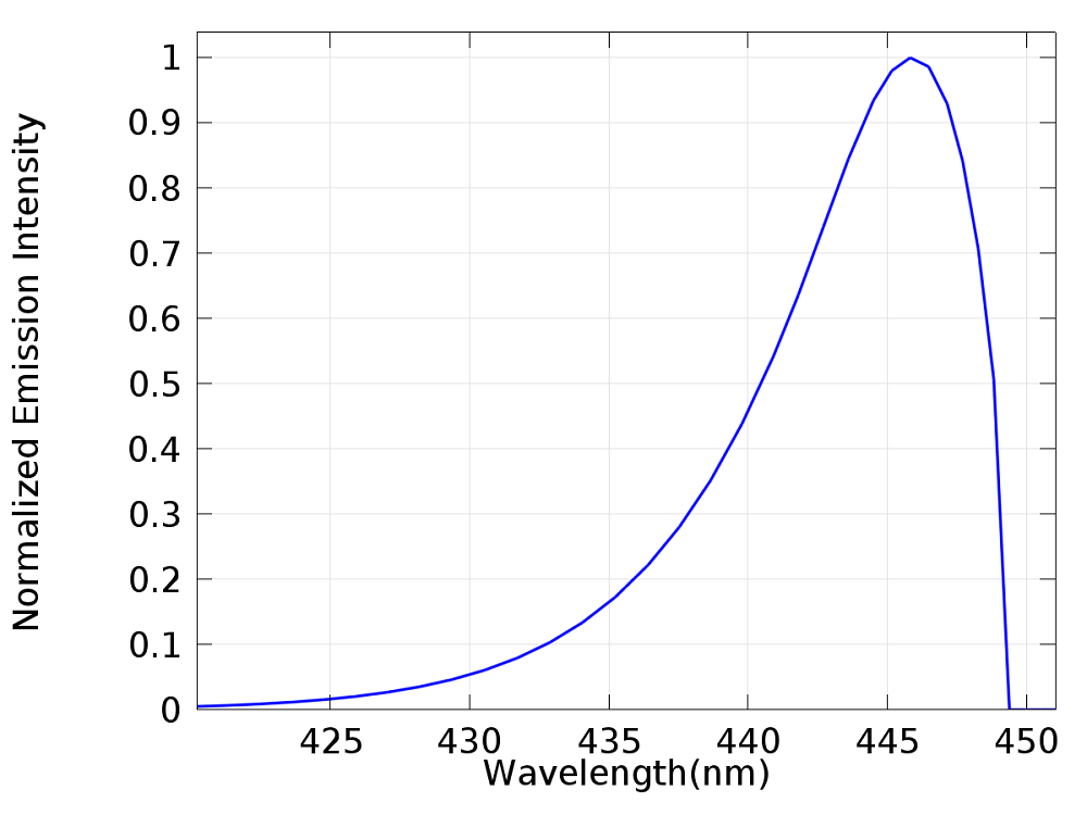
Calculated electroluminescence spectrum from the center of the InGaN layer.
Optimizing Efficiency of LED Light Output
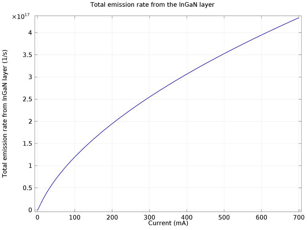
We can visualize the effects of LED droop by plotting the total rate of photon emission from the InGaN layer as a function of the driving current. Initially, the total emission rate increases almost linearly with current. However, after a few tens of mA, it curves over to follow a very sub-linear growth rate.
The sub-linear increase in the total emission rate as a function of driving current is characteristic of LED droop.
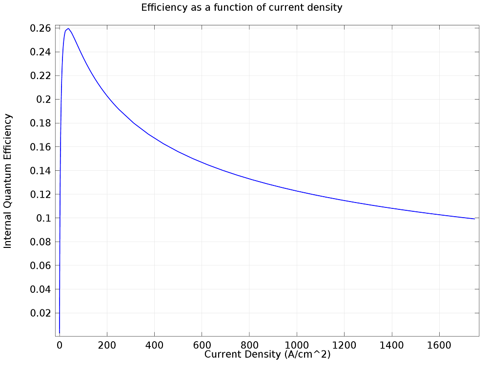
We assess the efficiency of the LED by considering the ratio of the total photon emission rate, integrated over the InGaN layer, to the carrier injection rate. This allows us to calculate the Internal Quantum Efficiency, which gives the probability that an injected carrier will radiatively recombine within the light-emitting InGaN region. As the lateral cross-sectional area of the double heterostructure device can be varied, it is useful to consider the Internal Quantum Efficiency as a function of current density, as shown in the diagram above.
There is a clear peak in the efficiency at current densities around 30 A cm-2, which can be explained by considering the carrier dynamics. At very low driving currents, the quasi-Fermi levels do not overlap with the band edges and the potential well is not preferentially occupied with carriers. In contrast, at current densities above ~100 A cm-2, the carrier density within the potential well is very high and other carrier-carrier interactions can reduce the fraction that radiatively recombine.
In addition to carrier-carrier interactions reducing the proportion of confined carriers that radiatively recombine, it is possible that the larger carrier injection rates associated with increased current densities reduce the proportion of carriers confined within the InGaN potential well prior to recombination. Additionally, Joule heating by increased currents could reduce efficiency, as electron energy that goes into heating the device cannot be used for light production. However, the effects of reduced carrier confinement probability and heating are not included in this simulation.
Although the exact mechanisms involved in LED droop are not fully understood, our multiphysics simulation has focused on the effects of non-radiative decay mechanisms. These mechanisms can reduce efficiency by decreasing the proportion of recombination events that emit photons. Carrier-carrier interaction effects are included using an Auger recombination model and impurity scattering effects are included using a Trap-Assisted recombination model. The screenshot below shows these two non-radiative features included in the Model Builder tree alongside the Optical Transitions feature, which calculates the radiative emission rate using a direct bandgap transition model.

Screenshot of the COMSOL Model Builder tree highlighting the included recombination mechanisms.
The Auger recombination — which requires carrier-carrier interactions within each band — has the most significant effect on the emission efficiency. The rate of Auger recombination is proportional to the cube of the carrier density, whereas the rate of direct radiative recombination is proportional to the square of the carrier density. This means that as the carrier density is increased, the relative rate of Auger recombination increases, reducing the fraction of carriers that recombine with the emission of a photon. Thus, the efficiency is lowered.
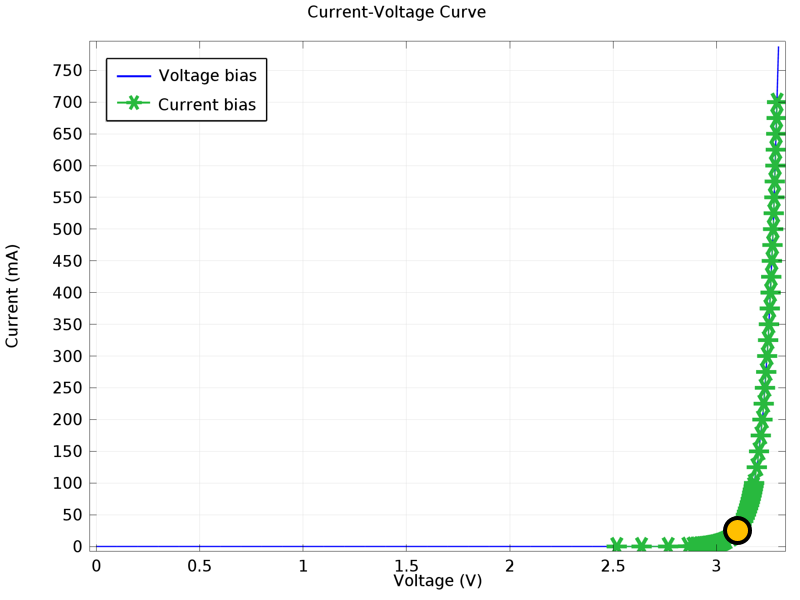
Current-voltage curve for the device. The blue line shows data obtained from a voltage driven study in which voltage boundary conditions were applied to the contacts and the resulting current was calculated. The green markers show data obtained from a current driven study in which the current was fixed at the p-contact and the resulting voltage was calculated. The yellow circle indicates the current range which corresponds with the peak in the Internal Quantum Efficiency.
The device is modeled with lateral dimensions of 200-by-200 μm. The peak of the Internal Quantum Efficiency corresponds to 10-30 mA of driving current, which is typical for LEDs of this size. Consideration of the current-voltage curve for the device, shown in the figure above, allows us to clearly visualize the consequences of LED droop. The device shows typical diode behavior, with a turn-on voltage of around 3.3 V. The blue line and green markers show the results calculated from a voltage driven and current driven simulation, respectively. The yellow circle indicates the range of currents over which the LED can be operated efficiently.
Because of LED droop, the LED is restricted to operating at currents just around the diode turn-on voltage. This means that in order to increase the total rate of photon emission without sacrificing efficiency, we must increase the area of the device. Eliminating or mitigating LED droop would allow the brightness of the LED to be increased simply by driving it with a larger current, without a reduction in efficiency. As less semiconductor material would be needed for a given light output, this would reduce the cost and environmental impact of LED lighting products.
Conclusions and Further Reading
Using the power of multiphysics simulation, we have investigated the emission characteristics and ideal operating range of an LED device. We saw the importance of non-radiative recombination mechanisms and how they contribute to LED droop in our model results. In combination with experimental results to validate which processes need to be included and the relative importance of each possible efficiency-reducing mechanism, simulation can be an important tool in enhancing product development activities.
- Download the model shown in this blog post: InGaN/AlGaN Double Heterostructure LED.
- Read more about the 2014 Nobel Prize in physics and recombination mechanisms in GaN-based LED devices:




Comments (1)
鹏 郑
February 27, 2025如果要计算EQE,是否要耦合电磁波频域模以计算出射光子数?