Silicon planar devices, imaging sensors, and microprocessors often include a metal-oxide-silicon (MOS) capacitor. To ensure that these devices perform as expected in an application, engineers can accurately analyze their designs using simulation. With the Semiconductor Module, an add-on product to the COMSOL Multiphysics® software, there are multiple methods to do just that…
Taking a Closer Look at MOS Capacitors
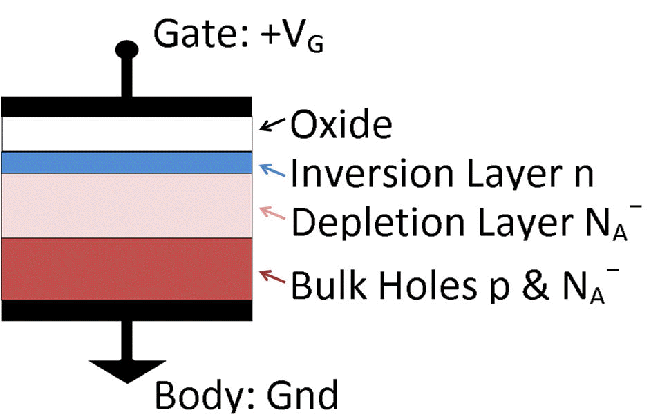
A MOS capacitor (MOSCAP) contains three main parts:
- A semiconductor body or substrate
- An insulator film
- A metal electrode (or gate)
There are two main types of MOSCAPs: surface channel and buried channel designs. The design used depends on the application.

A MOSCAP. Image by Brews ohare — Own work. Licensed under CC BY-SA 4.0, via Wikimedia Commons.
In general, MOS structures are used in silicon planar devices to generate capacitance measurements, helping engineers to understand the working principles of these devices. MOSCAPs specifically are used in charge-coupled devices (CCDs) for medical and imaging technology applications. Typically, they serve as components in MOS transistors, commonly used semiconductor devices found in integrated circuits and components like microprocessors.
To ensure MOSCAPs function properly, engineers need to predict their behavior. The Semiconductor Module, an add-on to COMSOL Multiphysics, provides multiple methods for analyzing MOSCAPs.
2 Ways to Simulate a MOSCAP
The 1D MOSCAP model used in these examples is grounded on the right endpoint and has an oxide-silicon interface at the left endpoint. To better study the oxide-silicon interface, engineers can refine the mesh at this point via a user-controlled mesh. There is also a uniform doping and Shockley-Read-Hall recombination applied throughout the modeling domain. In addition, to make the model setup process easier, engineers can use the material data for silicon that is available directly in COMSOL Multiphysics.
Using a model like this one, researchers can analyze MOSCAP behavior in many different ways, such as with the two methods briefly discussed below.
Tip: The methods featured here are explained with step-by-step instructions in the documentation for these examples, which is linked to at the end of this post.
Method 1: Voltage Sweep
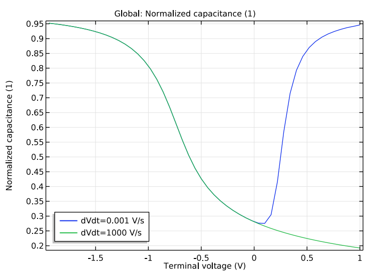
In the first example, the model domain is 1 mm thick and the MOSCAP is simulated using a voltage sweep with a Stationary study step for the initial condition as well as a Time-Dependent study step for the sweep.
When using this functionality, it’s possible to study the MOSCAP behavior under a linear voltage ramp. Here, the voltage ramp ranges from -2 to 1 V. It has a low-frequency slew rate of 10-3 V/s and a high-frequency slew rate of 103 V/s.
Method 2: Small-Signal Analysis
Engineers may also want to run a small-signal analysis to determine differential capacitance values at an array of DC bias points in a MOSCAP design.
As of COMSOL Multiphysics® version 5.3a, there are two features in the Semiconductor Module that can be used in semiconductor models. The first is the Semiconductor Equilibrium study step, which can be used to study systems in equilibrium and to produce initial conditions for nonequilibrium systems. There’s also the Quasi-Fermi level formulation, which helps engineers deal with highly nonlinear systems of equations when modeling semiconductor devices in extreme conditions, like very low temperatures.
![]()
The Semiconductor Equilibrium study step in the COMSOL® software.
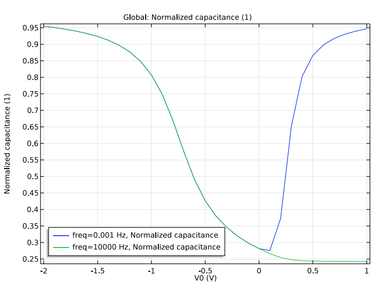
These features are demonstrated in the small-signal analysis model of the MOSCAP. As a result, this method can examine an array of linear DC bias voltages ranging from -2 V to 1 V. At the same time, it can account for a small-scale harmonic perturbation of 1 mV that has a frequency of 10-3 Hz for the low-frequency case and 104 Hz for the high-frequency case. The model used in this example has a domain thickness of 10 um.
MOSCAP Simulation Results
Both of these simulation methods can be used to calculate low- and high-frequency C-V curves, which are important for analyzing MOSCAP designs. You can see these curves in the images below for both versions of the MOSCAP model. Both methods generate similar C-V curve results.
C-V curves for the voltage sweep (left) and small-signal analysis (right).
We found that the behavior seen in both plots matches what is typically seen in textbooks, such as the plot in Reference 1 in the model documentation. As such, these models highlight the ability of the Semiconductor Module to reach an accurate solution when using alternative methods.
Next Steps
To try the examples discussed in this blog post, click the links below. Doing so will take you to the Application Gallery, where you can download the PDF documentation with step-by-step instructions.
Learn more about semiconductor simulation on the COMSOL Blog:


Comments (0)