
If you were to take apart almost any modern electronic product, you would find a printed circuit board (PCB). A closer look at this common component reveals a pattern of copper lines on its surface. These conducting lines can be created using a process called electrodeposition, which modifies device surfaces via electrochemical reactions. To enhance electrodeposition techniques for circuit board manufacturing, engineers can use numerical modeling.
Using Electrodeposition to Manufacture PCBs
In short, electrodeposition is an electrochemical process used to coat a substrate with another material. This versatile process is used for both decorative and functional purposes and is found in a variety of different fields, such as electronics, mining, and nanotechnology. One form of electrodeposition is electroplating, which is used to manufacture circuit boards.
Typically, PCBs are made of one or more layers of copper that are deposited onto or between a nonconductive substrate. The copper layers are separated into conducting lines or traces that enable signals to pass through the PCB. To form these patterned lines, engineers can electroplate copper into microcavities located on circuit boards.
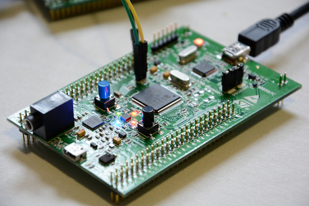
An example of a PCB. Image by AB Open. Licensed under CC BY 2.0, via Flickr Creative Commons.
Using electroplating to manufacture PCBs includes challenges. For example, variations in the copper plating rate across the PCB surface can cause performance issues and even device failure. To identify and prevent issues in the electroplating process, engineers can use the COMSOL Multiphysics® software and add-on Electrodeposition Module.
Analyzing Copper Electrodeposition in a Circuit Board Trench
The example discussed here models copper electrodeposition on a circuit board with a small trench or microcavity. A laboratory cell under potentiostatic control serves as the plating cell, and the anode is located close to the cathode. When deposition occurs, the cathode and anode boundaries move, making the simulation inherently time dependent. In addition, the copper deposition rate is nonuniform across the surface of the cathode.
The model is a benchmark model for electrodeposition and highlights the ability of the COMSOL® software to solve electrochemistry problems involving deformed geometries. Here, deforming geometries are used to analyze the plating process and how cavities affect the plating result. The use of a deforming geometry enables engineers to study the cathode boundary growth during the electroplating process.
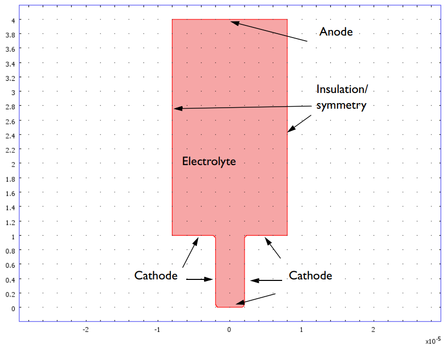
Geometry of the copper deposition model. The vertical walls represent the pattern on the master electrode and are insulating.
To solve this problem, engineers can use the built-in ALE method, which predicts the deformation or displacement of an object based on the underlying physics. Using the ALE method enables engineers to properly study the shape of the deposition in highly accurate electrodeposition models.
If you want to learn more about the model setup, including the work by E. Mattsson and J.O’M. Bockris that it is based on, check out the model documentation here.
Copper Electrodeposition Simulation Results
The copper deposition process is examined after 5 seconds have passed. At this time, there are substantial variations in the copper ion concentrations throughout the cell. Eventually, these variations may cause free convection within the cell, but this is not accounted for in this benchmark. We can see that the mouth of the trench begins to narrow, which is caused by the nonuniform thickness of the copper deposition.
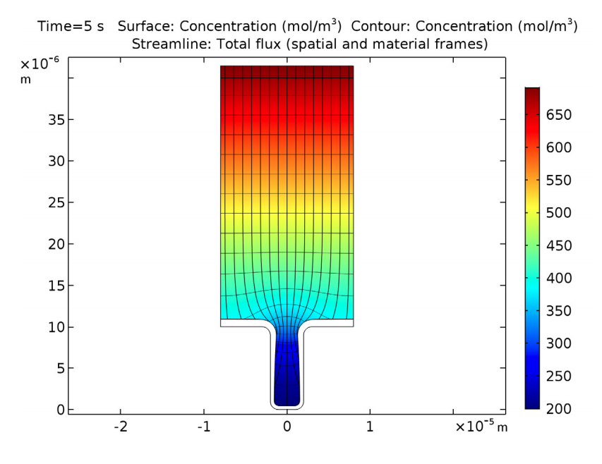
Copper ion concentrations, isopotential lines, current density streamlines, as well as cathode and anode displacement. The model shows symmetry along a vertical line located in the middle of the cell. This is good, since a nonsymmetric result indicates a poor mesh resolution.
The results below show that the top of the trench continues to narrow as time passes. This could harm the deposition quality, as trapped electrolytes can lead to corrosion in circuit board components.
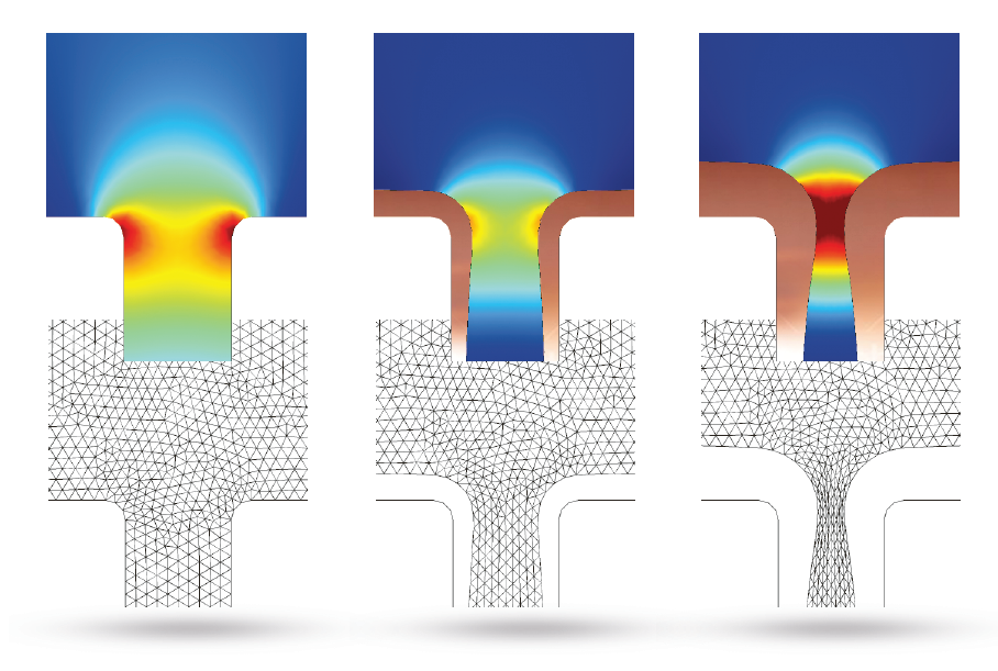
Image (top) and animation (bottom) showing the copper deposition over time. The top image also highlights the moving mesh used to solve this example.
The next plot examines the deposition thickness along a vertical cathodic surface. This graph provides another way to see that a nonuniform deposition is developing. This happens because of the nonuniform current density distribution, which is intensified by the depletion of copper ions along the cavity depth.
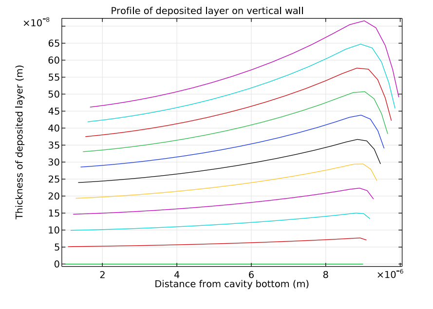
Deposition thickness along the vertical cathode boundaries. Each line in this plot represents an increment of 0.4 seconds in the range of 0.4 seconds–4.4 seconds.
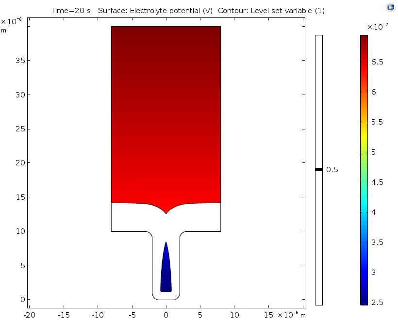
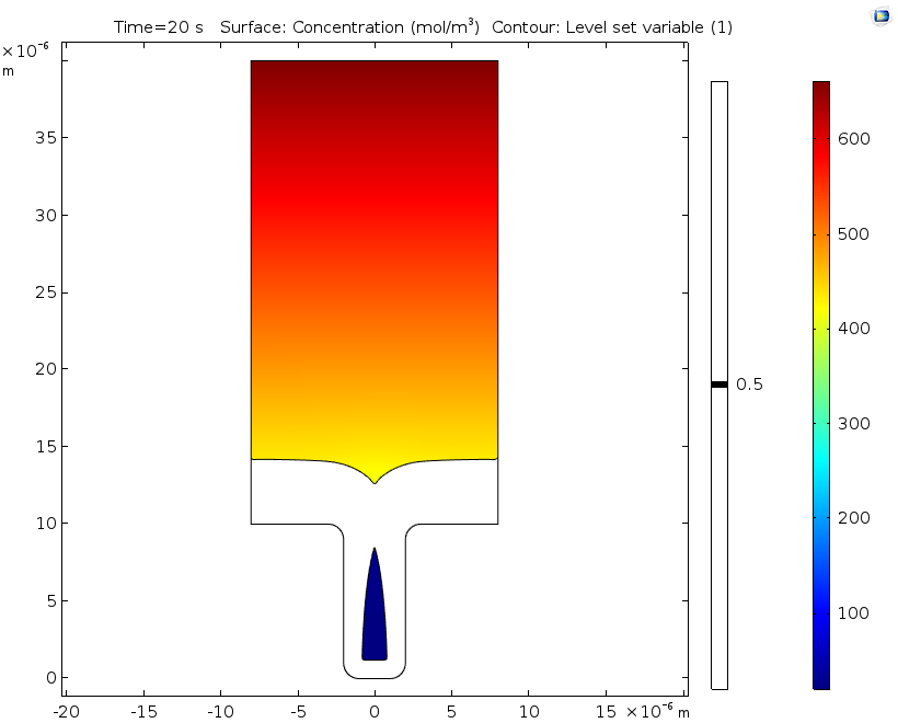
If desired, engineers can extend the time studied in this analysis by swapping out the ALE method for the level set method, as seen in this example. Doing so makes it possible to analyze deposition after the cavity is formed, since the level set method enables the study of topological changes. This extended analysis shows that the nonuniform deposition causes the formation of a potentially harmful cavity or void. In line with the previous results using ALE, it also shows substantial variations in the concentration of copper ions.
Electrolyte potential (left) and copper ion concentration (right) for a level set variable contour with a value of 0.5 after 20 seconds of deposition.
Overall, these results indicate that the current design may harm the deposition quality and cause corrosion and material waste. After pinpointing these potential issues via numerical modeling, engineers can enhance their designs…
Improving the Copper Electrodeposition Process with Simulation
Using models like the one described above, engineers can accurately analyze the electrodeposition process and test different operating parameters, applied potentials, and deposition surface geometries. In this way, they can find optimal electrodeposition parameters and improve the deposition uniformity, enabling them to more efficiently generate high-quality products.
The model featured in this blog post can be used as a starting point for achieving these goals. Engineers can tailor this simple example to their specific needs by accounting for the influence of other ions and testing more complicated geometries. To try it yourself, click the button below. Doing so will take you to the Application Gallery, where you can download the related MPH file and tutorial documentation.




Comments (2)
Adrian Schiffer
June 21, 2018Thats interesting! What i ask myself is, if it is possible to simulate the Conductive Anodic Filament (CAF). The processes are similar, so it should be possible to apply this to analyze this very common failure on PCBs… 🙂
Lautaro Gambino
June 29, 2020Hi,
I’m attempting to simulate deposition of nickel in nanocavities with a 3 electrode system, where the nickel ions comes form the electrolyte solution and make a cyclic voltammogram(CV) and chronoamperometry study. I’ve been using this app model and some others to get started with COMSOL, but i haven’t been successful in modeling a electrodeposition reaction where the source of ions comes from the electrolyte solution.
By any chance could you give me some guidance or know someone who can guide me in the electrodeposition module?
Thank you in advance,
Sincerly, Lautaro Gambino