
A frequent modeling situation encountered in wave electromagnetics modeling is to compute the scattering of light off of a structure patterned on top of a uniform dielectric substrate. In this blog post, we will present one way to model such situations in the COMSOL Multiphysics® software.
Background and Overview
The case we will consider here is of a small scatterer of light: a half-cylinder of gold patterned on top of a dielectric substrate. We are interested in the case of just a single scatterer, and we will assume that the illumination is from a beam of collimated light that is so much larger in diameter than the scatterer, so that it can be well approximated as a plane wave. The plane wave can illuminate the structure at an arbitrary angle and state of polarization. The dielectric substrate is assumed to extend infinitely in the negative z direction.
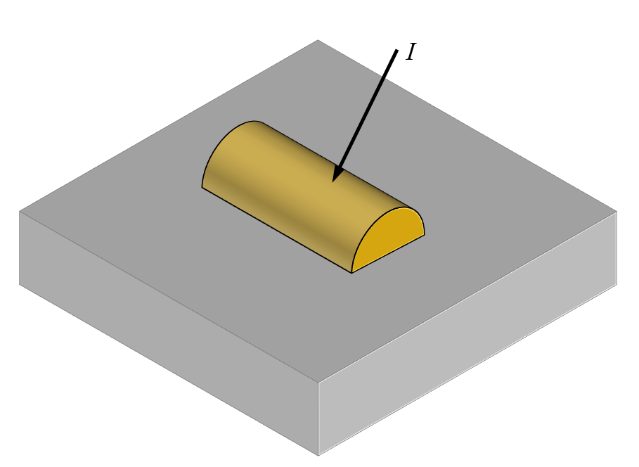
Light incident at an arbitrary angle on a single scatterer on a semi-infinite dielectric substrate.
Since we want to model just a single scatterer that represents a relatively small perturbation in a background field, it makes sense to use the Scattered Field formulation. This formulation requires that we enter a background electric field that would represent the solution to Maxwell’s equations in the absence of the scatterer. That is, we solve Maxwell’s equations in their frequency-domain form:
But write the total electric field as:
Rather than solving for the total field, we solve for the relative field, also often called the scattered field. The background electric field is the solution to Maxwell’s equations over the domains in question in the absence of the scatterer. For the simple case of an object in free space, the background field is simply a plane wave, as used in the RF Module benchmark example Computing the Radar Cross Section of a Perfectly Conducting Sphere, which compares the solution of this method against the analytic result. A similar example from the Wave Optics Module computes the scattering off of a gold nanosphere. One might be tempted to use the same approach for a dielectric half-space, but then the background field would be wrong.
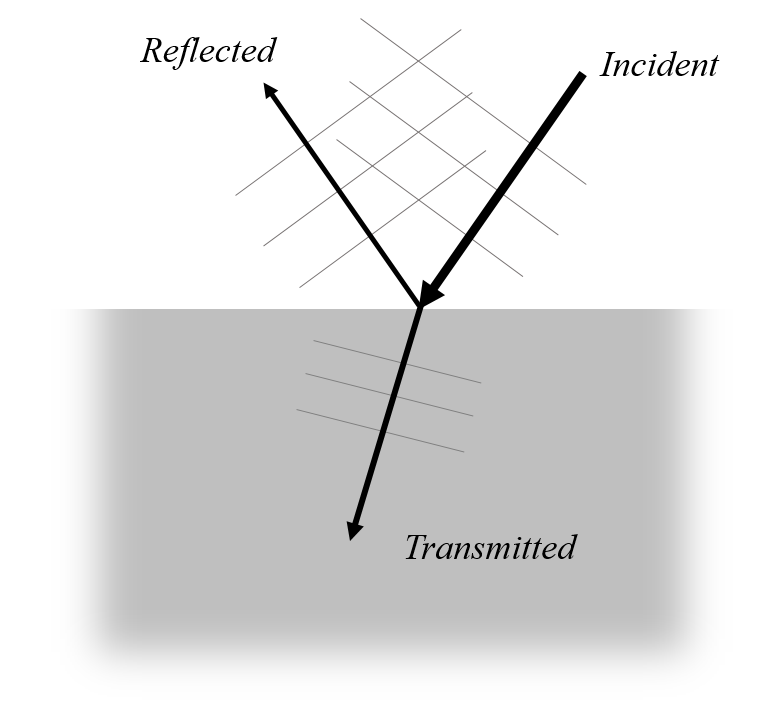
The electric field at a dielectric interface, absent any scatterer, is the sum of the incident, reflected, and transmitted plane waves.
For the case of a scatterer on a semi-infinite lossless dielectric substrate, the equation for the background field must incorporate the reflection and refraction at the interface. One approach is to compute the background field based upon a separate analysis and use that computed field as the background field. This approach is demonstrated in the Scatterer on Substrate example from the Application Gallery. However, here we will instead look at directly entering the background fields for a light incident upon a dielectric half-space by using the analytic solution.
Using the Fresnel Equations to Define the Background Field
The Fresnel equations, along with Snell’s law, describe the reflection and transmission of a plane wave of light when incident upon a flat interface between two materials of different refractive index. These Fresnel equations begin with the definition of the plane of incidence, which is a plane described by the vector normal to the surface between the two materials, and the wave vector of the incoming plane wave. The incident electric field can be decomposed into a component that is purely perpendicular to this plane, called an s-polarized or TE wave, and one that is purely parallel to this plane, called a p-polarized or TM wave. For example, circularly polarized light is the sum of a TE wave and TM wave of equal magnitude, but 90° out-of-phase with each other.
In the plane of incidence, we can use Snell’s law to relate the angle of the incident (\theta_i) and transmitted (\theta_t) light relative to the surface normal in terms of the refractive indices, n_a and n_b, of the two materials:
Then, the Fresnel equations give us the reflection and transmission coefficients for the TE- and TM-polarizations:
rr_{TE} = \frac{n_a \cos \theta_i – n_b \cos \theta_t}{n_a \cos \theta_i + n_b \cos \theta_t} \\
t_{TE} = \frac{2 n_a \cos \theta_i}{n_a \cos \theta_i + n_b \cos \theta_t} \\
r_{TM} = \frac{n_b \cos \theta_i – n_a \cos \theta_t}{n_b \cos \theta_i + n_a \cos \theta_t} \\
t_{TM} = \frac{ 2 n_a \cos \theta_i }{n_b \cos \theta_i + n_a \cos \theta_t}
\end{array}
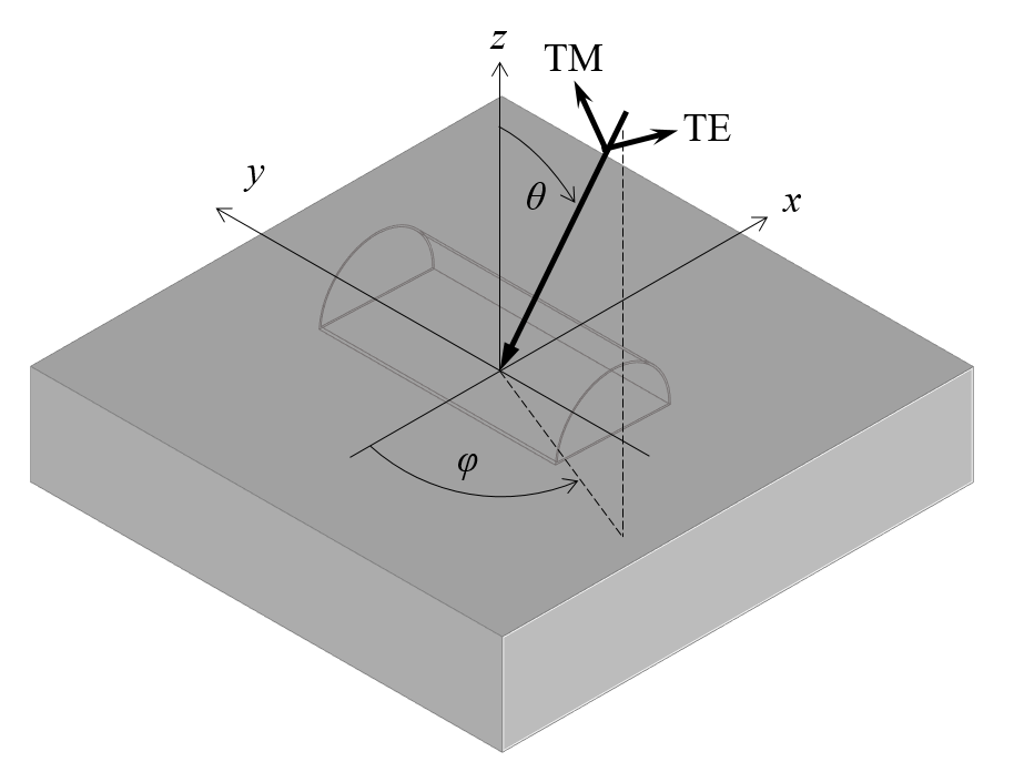
The TE- and TM-polarized components of the incident plane wave have to be transformed from the plane of incidence back to the global Cartesian coordinates.
We must next transform these from the plane of incidence back into the global Cartesian coordinates to get the k-vector of the incident and transmitted beam. Following the convention that the plane of the interface is the xy-plane, and the incident beam of wavelength \lambda_0 is propagating in the negative z direction, we define the angle of incidence \theta as the angle from the z-axis, and the angle \phi as the rotation about the z-axis starting from the negative x-axis, as shown in the figure above. This lets us define the k-vectors of the incident beam as:
And the transmitted beam:
The k-vector of the reflected beam, \mathbf{k}_r, is similar to the incident beam, but of opposite sign for the z-component.
Given an incident beam that is composed of both a TE- and TM-polarized component, E_{i,TE} and E_{i,TM}, the components of the electric field of the incident beam are:
And for the reflected components:
So, the total background field on the incident side is \mathbf{E}_{background} = \mathbf{E}_i + \mathbf{E}_r, and of the other side of the interface, the field is \mathbf{E}_{background} = \mathbf{E}_t, with components:
These expressions can be entered as sets of variables defined over different domains within the COMSOL Multiphysics® software, and used as the background field definition.
Sample Model and Discussion for Modeling the Scattering of Light
A sample model demonstrating this approach is set up and available via the link below. The electric field magnitude and the losses in a small half-cylinder of gold are plotted.
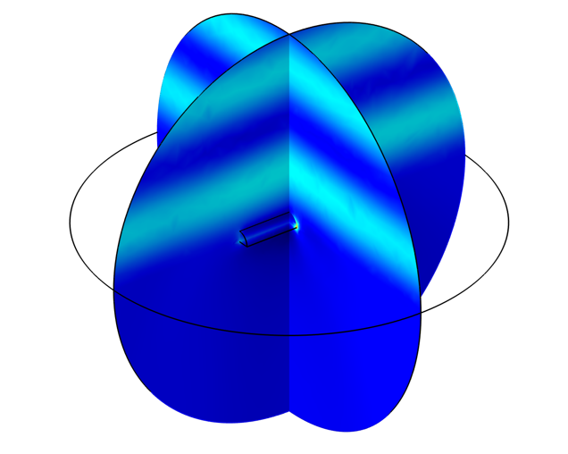
Electric field magnitude around a gold scatterer on a dielectric substrate.
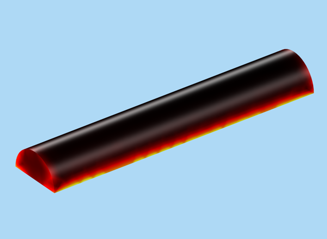
Losses in the gold scatterer.
Although this approach of entering the analytic background field is a little bit more work in terms of model setup, it is faster to run than the Scatterer on Substrate example, which first has to compute the background field. The merits of the latter approach would be when considering a case where the analytic solution is more difficult, or even impossible, to write out. So, for the case of a uniform dielectric substrate, this approach is likely always preferable.
Next Step
Try modeling a scatterer on a substrate using the analytic background field by clicking the button below.


Comments (18)
Tharindu Warnakula
April 19, 2020Hello Walter,
thank you for the great explanation. I have a question regarding multi-layer structures. It seems like this approach of calculating the reflected and transmitted fields would not work in such a situation since there would be fields due to multiple orders of reflection. Am I Correct? In that case, would I be better off just following the strategy from “scatterer on substrate” and solving for a background field numerically? Is there a way around that?
Tharindu.
Walter Frei
April 20, 2020 COMSOL EmployeeHi Tharindu, Yes, that’s correct, for a scatterer on a multi-layer substrate you’d be better (simpler) off numerically computing the background field.
Tharindu Warnakula
April 30, 2020Got it thanks Walter!
ziyang ye
February 18, 2021Hello Walter,
Thank you so much for your excellent explanation. I’m curious is there a way to calculate the BG field(analytical or numerical) if the incident light is an x-polarized Gaussian beam tightly focused on the dielectric substrate? Previous I try to do that in a similar way like “scatterer on substrate”. In full-field mode, I set an exciting port(constant power and paraxial Gaussian expression as electric field mode) but the output pattern of ewfd.Ex looks so weird. Could you give me hint to find a solution?
Best
Ziyang
Rabiul Hasan
May 26, 2021Hello Walter,
In the comsol file, for a given incident flux, electric field in the free space is calculated using the following equation: E = sqrt(Incident flux*Z0). However, original formula should contain a factor 2 i.e. E = sqrt(Incident flux*2*Z0). Because for a plane wave in free space, Intensity = E^2/2Z0. If the surrounding medium has a refractive index na then the formula for electric field should be modified by: E = sqrt(Incident flux*2*Z0/na). Can you please explain why factor 2 is missing in the example file?
Rabiul Hasan
Walter Frei
May 26, 2021 COMSOL EmployeeHello Rabiul,
Thank you for pointing this out. The file has been updated with the corrected factor.
Rabiul Hasan
May 31, 2021Dear Walter,
Thank you so much for responding on my query. Can I ask you another query? I have simulated the example model. What I found that for TE wave, y-component of the background field exist while for TM wave x-component exist. But if I want to simulate for TE waves with x-polarization then what should I change in the simulation setting? Please clarify.
Regards,
Rabiul Hasan
Juhwan Kim
July 15, 2021Hello Walter,
Thank you for the explanation. I have a question about the ‘scatterer on substrate’ model (or this new model). In this model, the substrate was assumed as a dielectric material. However, I want to simulate the case where this substrate is metal, for example gold. For this case, is it okay to remain the settings except for the material? My model gives the negative scattering cross section which is not what I want.
Juhwan Kim
Walter Frei
July 15, 2021 COMSOL EmployeeHello Juhwan,
Yes, you can use this approach, but you will need to think carefully about exactly what kind of field to apply, and exactly how to interpret the results.
Juhwan Kim
July 15, 2021Thank you so much for the reply. I have another question about the model. Is the negative scattering cross section a value that can be derived from a correct simulation? I simulated the ‘Scatterer on substrate’ model with wavelength domain 400 nm to 800 nm, and it shows negative scattering in a specific range.
Vikas Yadav
September 13, 2021Hello, Mr. Walter Frei
I just wanted to know that can we use Circular polarized light (RCP and LCP) in this field? , If yes please tell me how to set up it in this configuration above ? Also, How to calculate the scattering and absorption in this case ?, If I have to incorporate the equation then what are the equation that are gonna useful to calculate scattering and absorption cross-section ? This would be much more appreciated. Thank You.
Walter Frei
January 28, 2022 COMSOL EmployeeHello Vikas,
In the situation that you describe E_i,TE and E_i,TM would be equal in magnitude, but different in phase by 90°, i.e., a factor or +/-i.
A Z
May 29, 2023Hello Walter,
This example, and the Scatterer on Substrate (Application ID: 14699), are both great.
For context, I am looking to extend a model currently excited by a single plane wave to explore its behavior when excited by a complex field defined by the superposition of waves amenable to analytic representation.
I have a question about the difference between: a) defining (or computing) a background field and then using the scattered field formulation; and b) running a full field model with port excitation and the scatterer present. Specifically, when running the Scatterer on Substrate example, there are significant differences in the computed (magnitude, shape of the) fields in each case. This remains even after adding x- and y- periodicity in the scattered field (second) step of the first approach. This discrepancy is unexpected and raises questions about which solution best describes what is going on.
My questions: 1) what are possible causes of such discrepancy? 2) How can they be mitigated? 3) How can convergence of the two solutions be achieved?
Edit: Additional questions (after looking in detail at this example): 4) How critical is it to have a (non-zero) BG field defined in the PML region? 5) How critical is it to have listener ports that account for all transmitted modes in the full field implementation?
Thanks in advance!
Andres
UPDATE 2023.05.30
Regarding 5) above: I re-ran the Scatterer on Substrate model as full-field, including the gold scatterer, after automatically adding all diffraction orders from the source port. This added 16 diffraction order ports and 1 orthogonal polarization port associated with the source (Port 1 in model), as well as 40 diffraction order ports and 1 orthogonal polarization port associated with the listener (Port 2) port. This substantially improved the correspondence of the results with the scattered field formulation study (with x- and y- periodicity).
Rachel Keatley
May 30, 2023 COMSOL EmployeeHello Andres,
Thank you for your comment.
For questions related to your modeling, please contact our Support team.
Online Support Center: https://www.comsol.com/support
Nagarkoti
August 18, 2023Hello Walter,
Can we use the same analytical field, if we want to compute scattering by the hole (void) on the dielectric surface ?
Walter Frei
September 1, 2023 COMSOL EmployeeHello Anil, Yes, this would also work for voids.
Shubhanshi Sharma
March 6, 2024Hello Walter
Thanks for the excellent explanation. Can you tell me how to do the multiple decomposition of the scattered field in the case of substrate?
Shubhanshi Sharma
March 6, 2024Hello Walter
Thanks for the excellent explanation. Can you tell me how to do the multiple decomposition of the scattered field in the case of substrate?
Shubhanshi