From blood pressure sensors to electronic money cards, planar coils are widely used. Found on circuit boards, these coils are a good choice for inductive coupling, especially when space is limited. When designing these coils, it’s important to calculate both their inductance and resistance, as these factors play a key role in the device’s performance. To do just that, engineers can use layered shell functionality in the COMSOL® software, which enables them to model all coils on one plane.
Planar Coils: Advantages and Use Cases
Planar coils are named for the parts of the coil being primarily on the same plane (i.e., nearly flat). They take up less space than other inductors and thus are suited for any application with size restrictions, such as MEMS or implanted medical devices (like heart pumps). These coils can be fabricated on both rigid and nonrigid surfaces, which means they can be integrated onto printed circuit boards (PCBs) as well as flex circuits. Planar coils can also be batch fabricated, which results in a more cost-effective manufacturing process.
Due to these qualities, planar coils have many different use cases, mostly in the high-frequency range. A few examples include:
- Remote health monitoring (e.g., blood pressure sensors)
- Wireless power transfer (e.g., wearable/implantable medical devices)
- RF identification (e.g., electronic money cards)
- Induction heating (e.g., induction cooktops)
![]()
Planar coils can be used in PCBs for wearable technology, such as this fitness tracker.
When it comes to designing planar coils, there are two important factors: inductance and resistance. The latter should be extremely low (0 is ideal), since any resistance takes away from the coil’s efficiency. However, the inductance should be high so that the device can be coupled to another system. Determining the resistance and inductance can be complex, as you need to account for aspects such as the coil material, number of turns, and coupling between the electric and magnetic fields.
As a solution, engineers can compute resistance and inductance in planar PCB coils using electromagnetics simulation software. To make the modeling process more efficient, the AC/DC Module (an add-on to COMSOL Multiphysics) includes the Electric Currents in Shells interface, enabling you to analyze coil designs as (essentially) flat surfaces. As an example, let’s take a look at a simple planar coil model.
Modeling a Planar Coil as a Layered Shell with the AC/DC Module
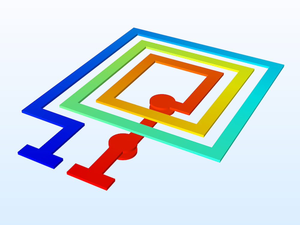
The model consists of a copper coil on a PCB. The coil itself has three turns; two vias; and two terminals, one of which provides the current while the other is grounded. The current starts at a terminal on the top layer. It then moves through the via to the bottom layer, underneath the turns, back up through another via to the top layer, through all of the turns, and finally to the grounded terminal. Traveling through the coil, the current generates the magnetic field, and the ratio of current to this field determines the inductance.

Geometry of the planar coil, showing the electric potential distribution.
Since the copper coil is very thin (only 0.1 mm thick with a width and height of 0.5 mm), it makes sense to model this coil via as a boundary, rather than as a part with volume. To do so, you can use the Electric Currents in Shells interface, available as of version 5.4 of the COMSOL® software, to model the coil geometry on one plane. In addition, you can use this physics interface, along with the Magnetic Fields interface, to compute the current flow and magnetic field and evaluate the resistance and inductance of the coil. This process consists of two parts:
- The Electric Currents in Shells interface computes both the lumped resistance and the surface current density throughout the coil. This interface solves for the currents flowing on boundaries.
- The Magnetic Fields interface uses the surface current density computed by the Electric Currents in Shells interface to calculate the magnetic field distribution in the volume around the coil.
Note that while this example is quite simple, you can use the same approach for different and more complex geometries. For all of the modeling details, check out the Planar PCB Coil tutorial. There, you can view step-by-step instructions and, if you have a valid software license, download the related MPH file.
Visualizing the Results of the Electromagnetics Simulation
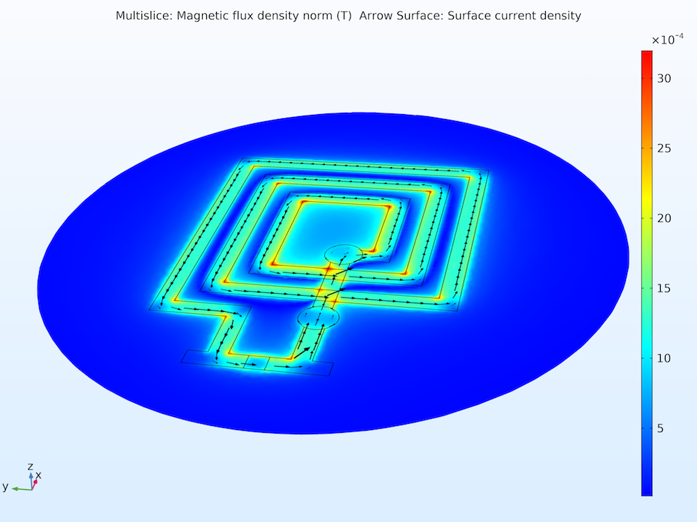
After running a simulation of the model, automatically generated results show commonly viewed quantities. These include the electric potential (shown above) as well as the magnetic field that is generated by the current flowing through the coil (shown below). In addition to these visual results, you can also calculate analytic results of interest; in this case, resistance and inductance. For this design, the inductance is 0.06 μH and the resistance is 21.6 mΩ.

The magnetic flux density around the coil (color plot) as well as the current density (arrow plot).
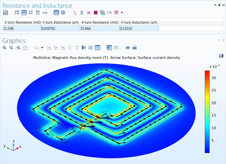
As you can see from this example, you can take advantage of the layered shell functionality in the AC/DC Module to model inductor coils as well as determine their resistance and inductance. Using the results of a simulation like this one, engineers can improve a coil design for a certain use case with ease, such as by adding more turns for a higher inductance. You can see this in the image below, where the inductance increases from 0.06 μH to 0.11 μH when a 4th turn is added.

The analytic results show a comparison of the resistance and inductance in a 3-turn coil vs. a 4-turn coil, and the visual results are shown for the 4-turn coil.
Next Steps
Try it yourself: Download the Planar PCB Coil example by clicking the button below. This will take you to the Application Gallery, where you can find the MPH file and documentation for the model.
Related Resources
- Read more about electromagnetics modeling on the COMSOL Blog:
- Watch an 18-minute video for an introduction to simulating electromagnetic devices


Comments (4)
sean mackenzie
February 12, 2019Is there some workaround to do the layered shell approach in earlier versions of COMSOL (e.g. 5.3a)?
Cesare Tozzo
May 27, 2019 COMSOL EmployeeAbout question above, yes, it is possible to use the former 5.3 interface “Electric current shell”, but you would need to have one interface per layer, and then to setup a more complex usage of selections that pays attention to couplings. With layered shell interface, the operations shown in step by step instructions highlight that how to use the same strategy independently of geometry (e.g. by repeating the the same model with a parametrized geometry using COMSOL standard geometric tools in the proper way, the model will just re-adapt to the new configuration returning the inducatance L as function of the current geometrical path).
Interact with us at support@comsol.com for any further help.
danny poincia
May 1, 2021How was the 0.1mm copper coil thickness specified in the model?
Sarah Vincent
January 21, 2026Is there a similar shell interface in the Magnetic and Electric Fields (mef) module ?