Perfect imaging refers to the idea of producing images with details below the diffraction limit, where even the smallest elements can be resolved to unlimited sharpness regardless of the wavelength of light being used. While just a theory 150 years ago, research has brought us closer to reality over the years. Now, by way of simulation, researchers at Cedint Polytechnic University of Madrid in Spain are taking it one step further.
Maxwell Fish-Eye Lens and the Diffraction Limit
Imaging systems have long been the subject of study for famous physicists like Maxwell, who proposed a fish-eye lens that uses a gradient index lens between a pair of points in space. The pair is defined by two opposite points laying on the spherical surface. Such a lens was supposed to be a “perfect imaging” system or, in other words, a system capable of focusing (imaging) the smallest detail from one point of its surface to another. Maxwell’s proposal was considered impossible to implement with an ordinary material with a positive index of refraction due to the diffraction limit. In practice, this means that in processes like photolitography, the size of features of an electronic device cannot be smaller than the wavelength of the light being used.
Below the Diffraction Limit with Ordinary Materials
In 2004 it was proven that an artificial material with a negative refractive index (also known as a metamaterial) could be used to overcome the diffraction limit. Later, in 2009, a breakthrough theory showed that an ordinary material could in fact be used to manufacture a Maxwell fish-eye lens. The latter approach intrigued professor Juan Carlos Miñano and his research team at Cedint Polytechnic University of Madrid. They decided to use simulation to prove the theory that the diffraction limit could be surpassed by designing a device with the equivalent optical properties of a Maxwell fish-eye lens, but with a different geometry: a spherical geodesic waveguide.
Spherical Geodesic Waveguide for Perfect Imaging
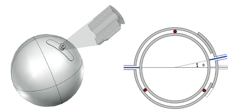
A spherical geodesic waveguide, which was designed by Miñano and his colleagues, is a very thin spherical metallic waveguide filled with a non-magnetic material (see figure below). At the moment, it’s still a proposed device that can be studied, optimized, and fabricated thanks to simulation. Miñano’s team couldn’t resort to geometrical optics, and therefore, to solve Maxwell’s equations with real-world accuracy, they decided to rely on COMSOL Multiphysics and the RF Module. The spherical geodesic waveguide model was designed and simulated using COMSOL by postdoctoral researcher Dejan Grabovickic from Miñano’s group.

The spherical geodesic waveguide with the drain port on top (left), where a cross section of the coaxial cable and its mesh are shown. The cross section (right) of the spherical geodesic waveguide including the drain port.
The spherical geodesic waveguide is designed for short-distance transmission and demonstrated super imaging properties: it can sense changes in the position of its receiver that are much smaller than the wavelength of the light being used. Super imaging could drastically reduce the size of integrated electronics, and as Dejan states in the IEEE Spectrum magazine insert, Multiphysics Simulation, it could allow for the production of integrated electronics that are “much smaller than what is the state of the art — something like 100 times smaller.”
Further Reading
- Catch the full details on this fascinating story of scientific ingenuity in the User Story Gallery: “A 100-Fold Improvement in Lithography Resolution Realized with a 150-Year-Old “Perfect Imaging” System“
- Read more user stories similar to this one in the IEEE Spectrum insert, Multiphysics Simulation
- For those of you interested in learning more about the theory behind and the implementation of the simulation set up by Dejan, I suggest you also read:


Comments (0)