
When it comes to creating the next generation of flat panel displays and solid-state area lighting, organic light-emitting diodes, or OLEDs, may be used to help. While recognized for its various advantages, this emerging technology suffers from some weaknesses that reduce its overall efficiency. One such example is light loss, which is partially caused by the plasmon coupling effect. Looking to reduce the effect’s prominence in OLED devices, researchers from Konica Minolta Laboratory turned to the COMSOL Multiphysics® software.
Shedding Light on an Innovative Technology: Organic Light-Emitting Diodes
What if airplane walls could appear transparent, offering an expansive view while flying high above the clouds? Now, imagine if these same lightweight windows could also double as interactive entertainment screens. Such advancements could translate into greater fuel and cost savings, while providing further space and comfort for passengers. With the help of an emerging technology — organic light-emitting diodes (OLEDs) — these ideas are becoming a potential reality.
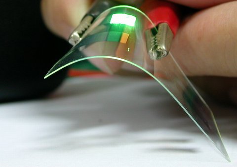
A flexible OLED device. Image by meharris. Licensed under CC BY-SA 3.0, via Wikimedia Commons.
OLEDs function similarly to LED lights, except that they use organic molecules to produce light. This newer technology is valued for its many favorable attributes, including being thin, flexible, lightweight, and bright. In general, OLEDs also feature a low operating voltage as well as low power consumption. Significant light loss, however, is an important concern, with only 20% of emitted light leaving OLED devices. This translates into a low outcoupling efficiency and low energy efficiency.
So what, you might wonder, is the cause of such light loss? Several factors can contribute. For instance, mismatches in the refractive index between the different OLED layers can result in total internal reflections. Another potential source is light coupling to surface plasmons at the metal cathode.
As a leader in the development of OLED lighting panels, Konica Minolta Laboratory noticed a lack of research behind the latter of these two cases — the plasmon effect. Using the RF Module in COMSOL Multiphysics, the team sought to analyze how plasmon coupling and structure impact the efficiency of OLEDs, presenting their findings at the COMSOL Conference 2015 Boston.
Using Simulation to Analyze Plasmon Loss in OLEDs
To begin, let’s take a closer look at the inner workings of an OLED. Such devices typically consist of two or more layers of organic material placed between two electrodes, namely the anode and cathode. All of these components are deposited on a substrate, which is often made of glass or plastic.
The diagram below provides an overview of the different individual layers. They include a metal (Ag) cathode; three organic layers: the electron transport layer (ETL), emitting layer (EML), and hole transport layer (HTL); a transparent anode (commonly made of an indium tin oxide, or ITO); and a substrate.
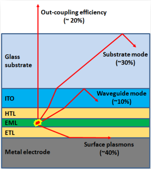
The structure of an OLED. Image by Leiming Wang, Jun Amano, and Po-Chieh Hung and taken from their COMSOL Conference 2015 Boston presentation.
The metal cathode, referred to as a metal electrode in the diagram above, is an important point of focus in plasmon loss. In fact, around 40% of the total emitted light ends up coupling to surface plasmons at this point — a significant percentage of the total emission. Reducing plasmon loss at the metal cathode is therefore an essential step when designing OLEDs.
Looking to do just that, the research team at Konica Minolta Laboratory used simulation to test the impact of incorporating a nanostructured or nanograting cathode structure into their OLED design. Here’s an overview of what they found…
Does Using a Nanograting Cathode Structure Improve OLED Efficiency?
When beginning their research studies, the team’s initial step was to analyze mode distribution and plasmon coupling in real space. To do so, they used a 2D simulation of a multilayer bottom-emitting OLED. This made it possible to easily identify the coupling of dipole emission into various light modes.
The initial set of results indicates that the waveguide mode does not contribute to light emission, as it essentially propagates toward the sides. With that in mind, the researchers shifted their attention to a wave featuring SPP wave characteristics, which you can see highlighted in the following figure. A surface plasmon polarization (SPP) wave is a surface wave that is confined to a narrow region at the boundary between the metal cathode and the neighboring electron transport layer.
The studies show that the excitation of the SPP wave at the cathode interface, and thus the coupling of dipole emissions into SPP, appears to be the main reason for plasmon loss. The findings ultimately confirmed the team’s decision to focus on evaluating plasmon loss and designing an alternate cathode structure.
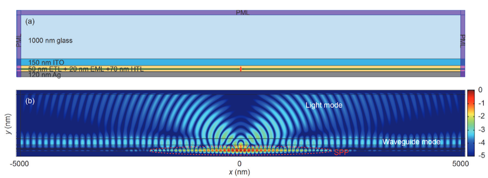
The simulation domain in 2D (top) and the field distribution of a multilayer OLED structure’s dipole emission (bottom). Images by Leiming Wang, Jun Amano, and Po-Chieh Hung and taken from their COMSOL Conference 2015 Boston paper.
The next item on the list was to measure the plasmon coupling effect for both flat and nanograting cathode structures. Creating electromagnetic models of the plasmon coupling effect at the metal cathode was a required step for the analysis. In an effort to focus specifically on the plasmon effect, the team used a simple model representing an Ag/EML structure featuring two layers. The finite element method (FEM) model enabled the researchers to simulate optical effects resulting from arbitrary subwavelength structures, which can be rather difficult to achieve through analytical simulations.
From the results, it is possible to draw a comparison between the dipole emission for a flat interface and a nanograting interface. The flat interface model (shown in the image below on the top) illustrates that the dipole emission is primarily coupled to the SPP wave, with just a small amount radiated out as usable light. On the other hand, SPP coupling is greatly suppressed when using a nanograting interface (shown in the image below on the bottom). Such findings suggest that using a nanostructured cathode can help significantly reduce plasmon loss. Before drawing any final conclusions, however, the team wanted to compare the two structures in a few other ways.
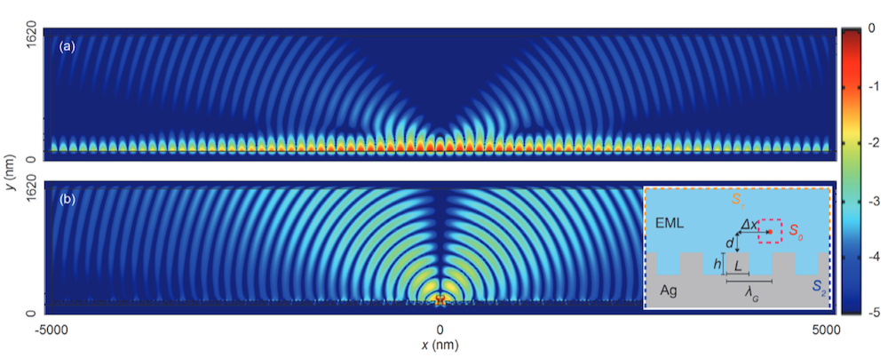
A field distribution simulation of a dipole emission for the two-layer OLED structure with a flat (top) and nanograting (bottom) interface. The insert, located in the bottom right-hand corner, depicts the structural parameters of the nanograting cathode. Images by Leiming Wang, Jun Amano, and Po-Chieh Hung and taken from their COMSOL Conference 2015 Boston paper.
For further insight into the structures, a power flow analysis was performed. The researchers were able to use the results found here to calculate the partition of total emission power into the light mode and plasmon mode. The results from this study refined the team’s earlier research by suggesting that to significantly reduce plasmon loss when using a nanograting structure, the cathode and emission layer must be less than 100 nm apart from one another.
The simulation studies up until this point involved the use of 2D models. 3D models, however, are superior for characterizing the isotropic nature of OLED light. The researchers therefore opted to add 3D simulations of OLEDs into the mix. As depicted by their results, strong field intensity exists in the cross-sectional xy-plane at the flat interface, confirming that strong SPP excitation occurs in the flat structure. The findings also reiterate that coupling to SPP is negligible for the nanograting structure.
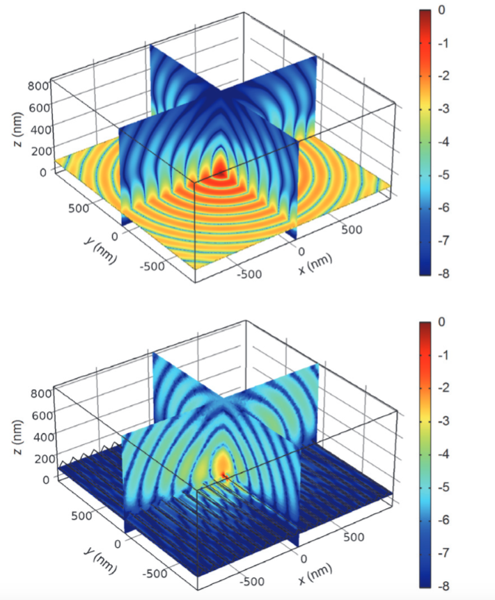
3D field distribution simulations of a dipole emission in an OLED model with a flat (top) and nanograting (bottom) interface. Images by Leiming Wang, Jun Amano, and Po-Chieh Hung and taken from their COMSOL Conference 2015 Boston paper.
Optimizing a Nanograting Cathode Structure with a Parametric Study
Building off their initial research studies, the team additionally sought to analyze the influence of size, shape, and nanograting period on the plasmon loss reduction. This translated into running parametric studies to optimize the nanograting cathode structure and see how structural changes affect plasmon loss. Here, we’ll focus on one such study, which looks at the grating structure’s effect on the overall plasmon reduction.

Left: The average relative plasmon loss (the plasmon loss with the grating relative to the plasmon loss with the flat surface) as a function of two different grating geometrical parameters: pitch height (on the x-axis) and pitch duty ratio (on the y-axis). Here, the pitch duty ratio is the quotient of the grating post width and the grating period. Right: Plotting the corresponding standard deviation of the wavelength averaging. Images by Leiming Wang, Jun Amano, and Po-Chieh Hung and taken from their COMSOL Conference 2015 Boston presentation.
The studies show that smaller pitch duty ratios lead to larger reductions in plasmon loss (represented by the darker colors in the figure above on the left). The dark colors in the right figure represent parameter combinations with a small wavelength variation. Therefore, the encircled common darker cells in the bottom-right corners of the figures indicate the optimal structure configuration for both reducing plasmon loss and having broadband performance. In fact, the circled cell generates an approximate 50% plasmon loss reduction over a broadband emission. This serves as additional proof that an optimized nanograting cathode structure can improve OLED efficiency.
There’s a Bright Future Ahead for OLED Devices
The simulation studies highlighted here mark a pivotal point in OLED research, with the mode distribution and plasmon coupling of OLEDs visualized in real space. The research findings provide opportunities for further innovative research into the design and optimization of the technology. As the efficiency of OLEDs continues to improve, their widespread commercial use will increase.
Learn More About Simulating Lighting Technology in COMSOL Multiphysics®
- Read the paper: “Simulating Plasmon Effect in Nanostructured OLED Cathode Using COMSOL Multiphysics“
- We’ve previously blogged about the role of simulation in optimizing light sources. Take a look at some examples:


Comments (1)
Rimeh Sassi
June 7, 2024can i help me
I have a multilayer OLED structure (ito/NPB/Alq3/NPB/BCP/Ca) I want to see the optical properties of this structure (radiance, electroluminance (EL) and luminance. In our work I do all the geometric parameter adjustments, material