
Electrically erasable programmable read-only memory (EEPROM) is a type of nonvolatile memory that enables users to repeatedly store and erase small amounts of data by applying a voltage pulse. EEPROM is often used as a storage medium in computers and mobile devices and has applications in devices like microcontrollers. To analyze the designs of EEPROM devices, engineers can turn to semiconductor simulation.
Improving Memory Devices: The Journey from ROM to EEPROM
EEPROM comes from a long line of increasingly improved memory devices. For instance, an early version of this type of memory, with a much shorter acronym, was read-only memory (ROM). While there were benefits, a main drawback of ROM was that it couldn’t be reprogrammed or rewritten.
To address this and other shortcomings, scientists created programmable read-only memory (PROM), which could be programmed with a special tool after creation. However, you could only program a PROM device once. This issue was tackled with the erasable programmable read-only memory (EPROM) design iteration, which enabled engineers to erase data themselves using UV light. While this was a solid improvement, EPROM chips had to be removed from a device in order to be reprogrammed.
That’s where EEPROM comes in. When compared to EPROM, EEPROM is superior because it can be reprogrammed with voltage pulses and the chip doesn’t need to be removed during the process. EEPROM tends to be slow, so a faster type of EEPROM called flash memory was also developed.
Some of the drawbacks of EEPROM are that it can only be rewritten a limited amount of times and, when removed from a power source, it will not store data indefinitely.
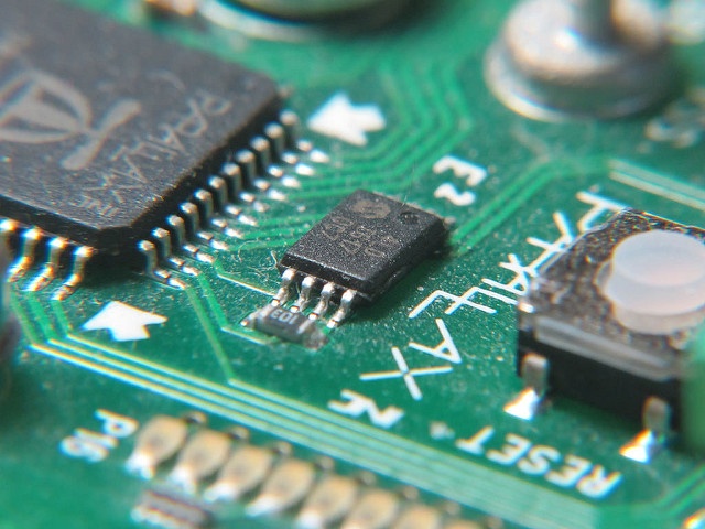
A surface-mounted EEPROM device. Image by Micah Elizabeth Scott — Own work. Licensed under CC BY-SA 2.0, via Flickr Creative Commons.
To study an EEPROM device, including its programming and erase cycle and its current and charge characteristics, you can simulate it via the COMSOL Multiphysics® software and the add-on Semiconductor Module. Check out the next section for an example.
Analyzing an EEPROM Device with Semiconductor Simulation
The floating-gate EEPROM example discussed here is based on work by A. Concannon, S. Keeney, A. Mathewson, and C. Lombardi (Ref 2. in the EEPROM tutorial documentation). The model geometry, seen below, has a total length of 1.8 μm and includes two electrically isolated gates: a floating gate and a control gate.
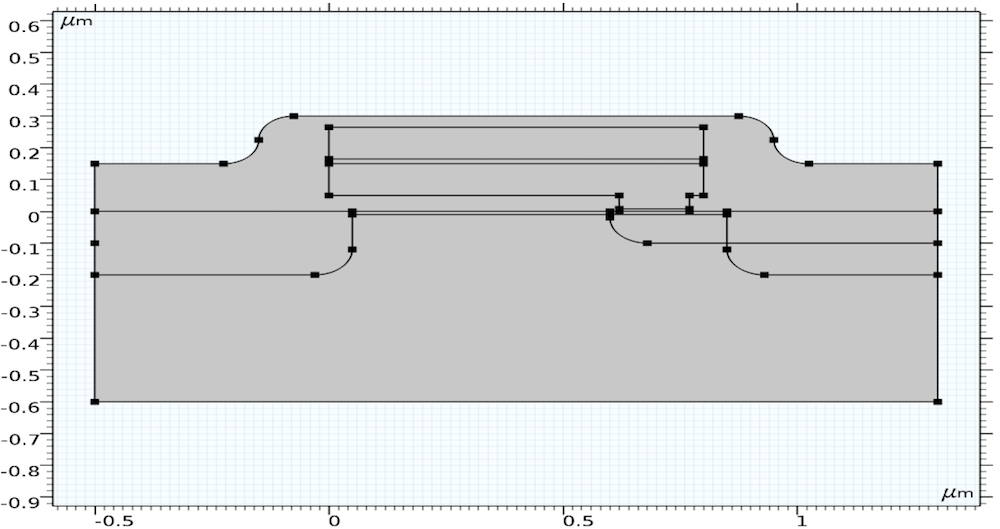
EEPROM model geometry.
In short, the program and erase cycle begins with the application of an initial voltage pulse to program the EEPROM device. Using this model, you can see that this pulse causes the electrons to tunnel across the tunnel barrier and accumulate on the floating gate, which stores the charge.
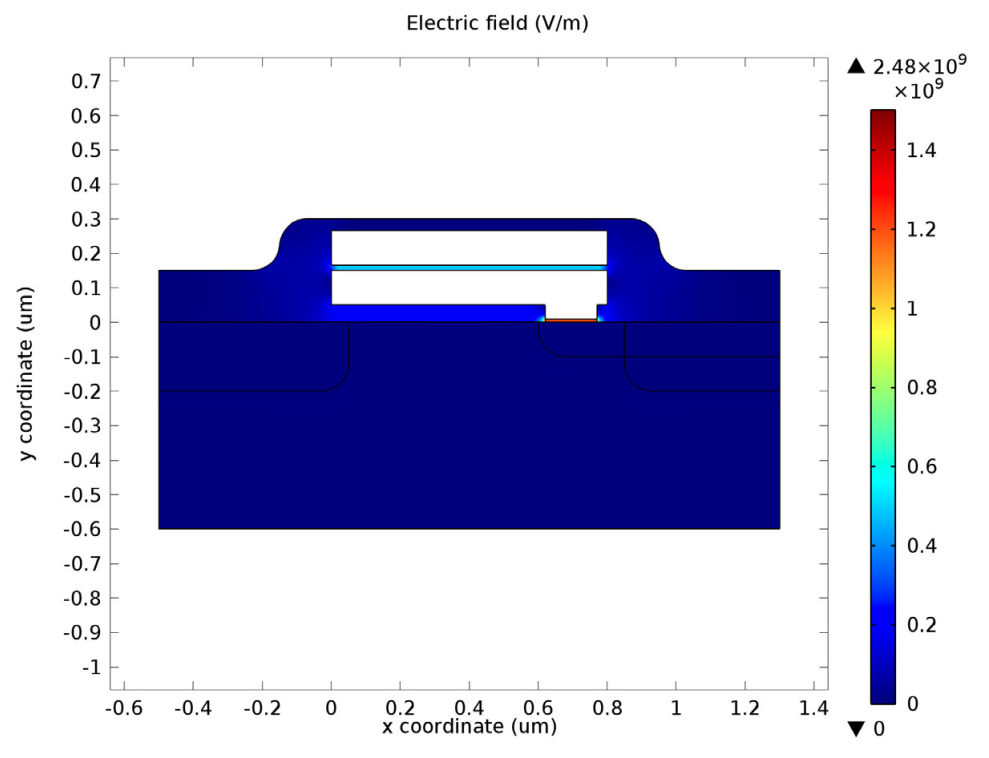
The electric field during the control voltage pulse that programs the EEPROM device. Here, you can see that the electric field is concentrated within the tunnel barrier.
To erase data from an EEPROM device, a negative pulse is applied, which causes the electrons to tunnel back out and return the floating gate to near its original state. With the COMSOL® software, you can simulate this program and erase process and calculate many different EEPROM device characteristics.
Examining an EEPROM Device
First, you can look at the results of a stationary study comparing the current-voltage (I-V) characteristics for a charged (programmed state) and uncharged (erased state) floating gate. As expected, no current flows between the source and drain before the device reaches the threshold “turn-on” control voltage. As the control voltage surpasses this threshold, more current can flow for the given source-drain voltage. A stored charge alters the threshold voltage, which in turn changes the source-drain I-V curve, as shown in the figure below.
Using the source current information gained from this study, it’s possible to determine if the floating gate is storing a charge. For instance, a control voltage of 1 V would yield no current in the erased configuration and a current of around 0.5 μA when charged to -2 x 10-15 C.
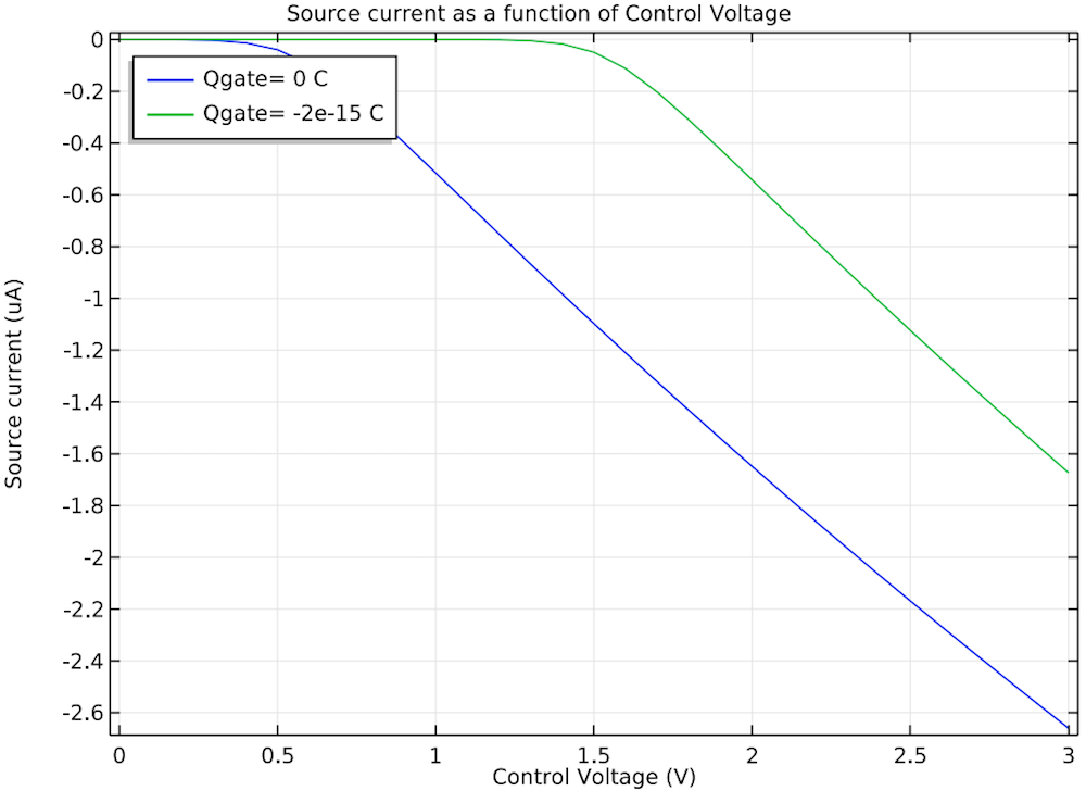
Source current versus control voltage when there is a fixed drain voltage of 10 mV. The blue line represents the device in its erased state and the green line represents the device in its programmed state.
The next two plots show the results of the time-dependent studies, which enable engineers to analyze the effects of the transient voltage pulses that allow the device to be programmed and erased over time.
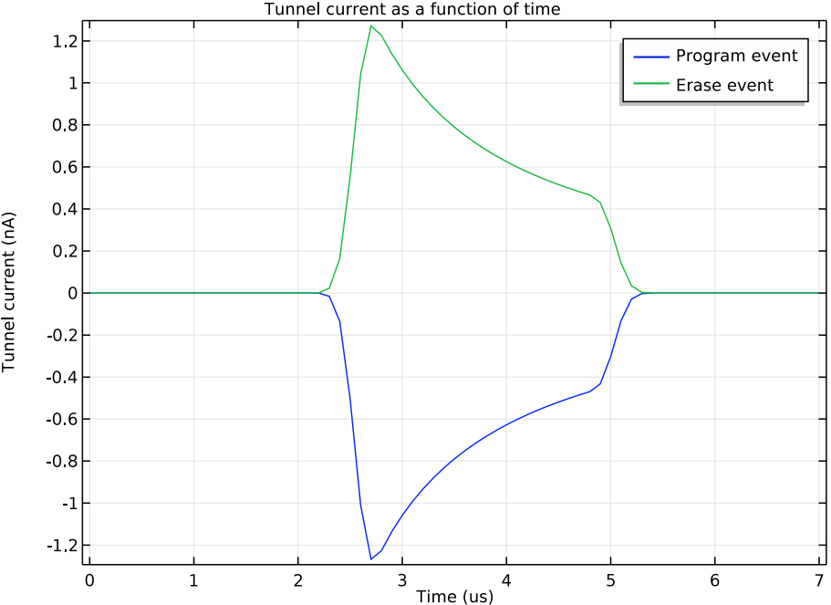
In the left plot below, you can see the tunnel current over time for both the program and erase events. The electrons tunnel into the floating gate during the program event and cause a negative conventional current. During the erase event, these electrons tunnel back out of the floating gate, causing a positive current that is equivalent in magnitude to the program event.
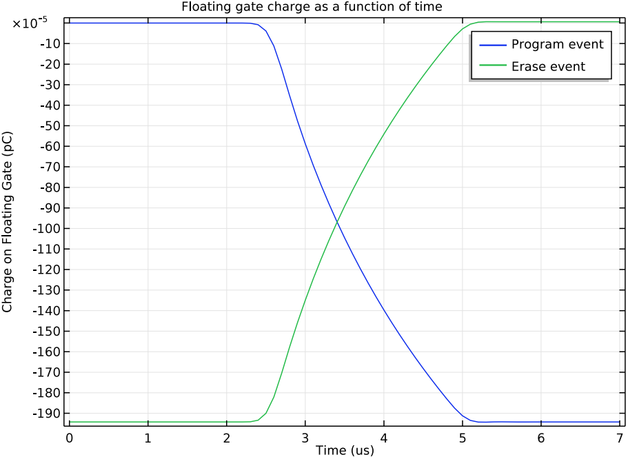
The right plot below shows the stored charge on the floating gate (which is caused by electrons tunneling through the tunnel barrier) as a function of time for both events. Here, the program event causes a negative charge to accumulate on the floating gate, while the erase event returns the charge to zero. These results are expected and help to confirm the validity of the semiconductor simulation.
The tunnel current (left) and the charge in the floating gate (right) as a function of time for the program (blue) and erase (green) events.
Next Steps
As demonstrated in this example, combining COMSOL Multiphysics and the Semiconductor Module enables you to accurately calculate and visualize the current and charge characteristics of a floating-gate EEPROM device. Want to give this example a try? Head to the Application Gallery via the button below to download this example and the related MPH file.
Learn about other uses of semiconductor simulation in these blog posts:




Comments (0)