Photonic Crystal
Application ID: 14703
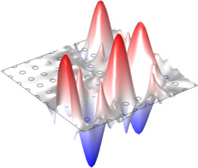
Photonic crystal devices are periodic structures of alternating layers of materials with different refractive indices. Waveguides that are confined inside of a photonic crystal can have very sharp low-loss bends, which may enable an increase in integration density of several orders of magnitude. This is a study of a photonic crystal waveguide. The crystal features a grid of GaAs pillars. Depending on the distance between the pillars, waves within a certain frequency range will be reflected instead of propagating through the crystal. This frequency range is called the photonic band gap. When some of the GaAs pillars in the crystal structure are removed, a guide for the frequencies within the band gap is created. Light can then propagate along the outlined guide geometry.

This model example illustrates applications of this type that would nominally be built using the following products:
however, additional products may be required to completely define and model it. Furthermore, this example may also be defined and modeled using components from the following product combinations:
The combination of COMSOL® products required to model your application depends on several factors and may include boundary conditions, material properties, physics interfaces, and part libraries. Particular functionality may be common to several products. To determine the right combination of products for your modeling needs, review the Specification Chart and make use of a free evaluation license. The COMSOL Sales and Support teams are available for answering any questions you may have regarding this.


