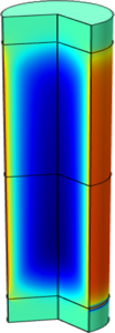
Surface Trapping in a Silicon Nanowire Gate-All-Around Device
Application ID: 19703
A gate-all-around MOSFET consists of a nanowire with a gate electrode wrapped around the circumference. Since the entire nanowire forms the channel, this configuration provides the best possible electrostatic control of the channel and offers a good candidate for the miniaturization of MOSFETs.
This model analyzes a silicon nanowire gate-all-around device, with different trap densities at the gate surface. The effect of the traps is to shield the electric field from the gate and thus increase the threshold voltage for opening the channel.
This model requires the Semiconductor Module.

This model example illustrates applications of this type that would nominally be built using the following products:
however, additional products may be required to completely define and model it. Furthermore, this example may also be defined and modeled using components from the following product combinations:
The combination of COMSOL® products required to model your application depends on several factors and may include boundary conditions, material properties, physics interfaces, and part libraries. Particular functionality may be common to several products. To determine the right combination of products for your modeling needs, review the Specification Chart and make use of a free evaluation license. The COMSOL Sales and Support teams are available for answering any questions you may have regarding this.


