The Application Gallery features COMSOL Multiphysics® tutorial and demo app files pertinent to the electrical, structural, acoustics, fluid, heat, and chemical disciplines. You can use these examples as a starting point for your own simulation work by downloading the tutorial model or demo app file and its accompanying instructions.
Search for tutorials and apps relevant to your area of expertise via the Quick Search feature. Note that many of the examples featured here can also be accessed via the Application Libraries that are built into the COMSOL Multiphysics® software and available from the File menu.
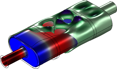
This model describes the pressure wave propagation in a muffler for an internal combustion engine. The purpose of the model is to show how to analyze both inductive and resistive damping in pressure acoustics as well as coupling the fluid to the surrounding elastic shell structure of the ... Read More
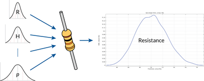
This example demonstrates how to apply the Uncertainty Quantification (UQ) Module in COMSOL Multiphysics to analyze the performance and reliability of a simple resistor. Small variations in material properties, geometry, and manufacturing processes can significantly impact the resistance ... Read More
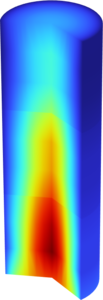
This model simulates a cylindrical furnace with isotropic scattering. It validates the use of the Discrete Ordinates Method for 2D axisymmetric cases, comparing the results with the highly accurate Monte Carlo method. The setup and reference Monte Carlo values are given in: R .P. Gupta, ... Read More
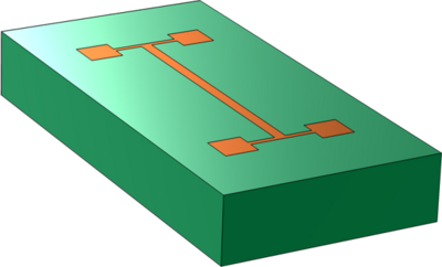
This model shows how to define a frequency-domain analysis of heat transfer. The 3-omega method uses the Cahill's equation to approximate the thermal conductivity of a sample from the measured temperature of a metal strip placed on top of it and subject to oscillating heating. The 2D ... Read More
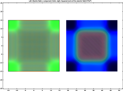
When two coherent light beams intersect, an interference pattern appears. If this occurs in a material that is sensitive to light, with intensities greater than a certain exposure threshold, the interference pattern is recorded in the material as a modulation of the refractive index and ... Read More
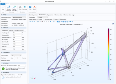
The reliability of a bike frame can be estimated by analyzing the structural stress subjected to different load cases. This app leverages LiveLink™ for SOLIDWORKS® to interactively update the geometry while computing stress analyses. Using this app, you can easily test different ... Read More
This model computes the trajectory of an ion in a uniform magnetic field using the Newtonian, Lagrangian and Hamiltonian formulations available in the Mathematical Particle Tracing interface. Read More
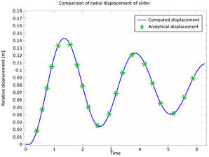
This model illustrates the modeling of slider motion caused by a base rotation. The motion of the slider is analyzed under various forces such as inertia force, centrifugal force, spring force and damping force. The prismatic joint, which is used to connect the two components, is spring ... Read More