2D/3D Design and Evaluation of a TE Single Mode Si-on-SiO2 Waveguide for Mid-IR CO2 Sensing Purposes
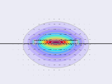
In this work, a 2.8x0.22 μm^2 silicon strip waveguide (n = 3.43 @4.234 μm) on a silica substrate (n = 1.38 @4.234 μm) and a superstrate with n = 1 was designed and evaluated through 2D (i.e., mode analysis), and 3D (i.e., wave propagation) analysis to strengthen the interaction between radiation and surrounding environment. By removing the superstrate, the evanescent field extending from the core of the waveguide can be used to interact directly with the gas molecules for sensing purposes. The waveguide is developed for an operating wavelength of 4.234 μm where a strong carbon dioxide (CO2) absorption line is localized with an absorption cross-section of 5.07x10⁻²¹ cm^2/molecule. A 3D sketch of the above-mentioned structure in shown in Fig. 1. The mode analysis performed to calculate the waveguide’s effective index of the Transverse Electric (TE) fundamental mode showing the strongest evanescent field intensity by optimizing both the width and thickness of the waveguide core. For this task, the Electromagnetic Waves, Frequency Domain (ewfd) interface within the Wave Optics branch was employed. The electric field profile resulting from this analysis is shown in Fig. 2. The effective index of 1.7483, shown in Fig. 2, was calculated for a waveguide’s core width of 2.8 μm and for a thickness of 0.22 μm by considering an operating wavelength of 4.234 μm. The dispersion curve was also retrieved showing a TE single mode behaviour of the overall structure for a waveguide’s core width in the 2-2.9 μm range. After that, a wave propagation study was carried out to evaluate the Poynting vector’s modulus inside the structure employing the Electromagnetic Waves, Beam Envelopes (ewbe) interface within the Wave Optics branch, and the results are shown in Fig. 3. The results shown in Fig. 3 indicate a maximum value of 11.3x10¹¹ W/m^2 for the Poynting vector’s modulus, and a constant trend along the direction of propagation. Finally, to further enhance the interaction between radiation’s evanescent field and the surrounding environment, an array of 34 block elements having the same width and thickness of the waveguide’s core and a depth of 150 nm with n = 1 was created along the structure to develop a periodic (i.e., with a period of 300 nm) waveguide structure able to operate below the reflection regime and so in the sub-wavelength one. Also in this case, the Poynting vector’s modulus inside the sub-wavelength waveguide structure was evaluated, and the results are shown in Fig. 4. The sub-wavelength waveguide structure was compared with the strip one in terms of Poynting vector’s modulus. The results shown in Fig. 4 indicate a maximum value of 7.25x10¹¹ W/m^2 for the Poynting vector’s modulus. Although this value is smaller than the one retrieved for the strip waveguide, the enhancement in terms of interactions between the radiation and the surrounding environment in the sub-wavelength structure allows a more efficient implementation for gas sensing applications. In fact, the guided TE mode directly interacts with the CO2 molecules within the 34 block elements each 150 nm deep with n = 1.

Download
- melchiorre_9571_poster.pdf - 1.09MB


