Study of Direct Wafer Bonding Process Based on Coupled Structural Deformation and Fluid Dynamics
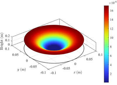
Wafer bonding technology has become a crucial process in 3D IC integration, particularly as a key method for monolithic integration where Through-Silicon Via (TSV) technology is not used [1]. However, due to the intricate mechanical stress and interconnect reliability issues associated with 3D IC stacking technology, conducting detailed simulation analyses before manufacturing is essential to optimize design parameters and ensure robust performance. This study utilizes COMSOL Multiphysics to conduct a comprehensive simulation of the wafer direct bonding process, focusing on the fluid-structure interaction (FSI) using the basic PDE module. The COMSOL PDE basic module was selected for its flexibility and ease of control, allowing for custom definitions and a solution of coupled PDEs tailored to the unique requirements for wafer bonding. This flexibility is crucial for accurately capturing the intricate interactions between structural mechanics and fluid dynamics in the wafer bonding process. In this study, the actual wafer structure was simplified to a 750 micron thick plate, with the bonding energy serving as the driving force to establish a fluid-structure interaction model. Using the PDE module in COMSOL Multiphysics, the mechanical and fluid equations were solved through general-form PDEs [2]. Specifically, the structural mechanics of the wafer was modeled using small-deformation theory, which captures the elastic behavior of the thin plates under bonding forces. Moreover, the fluid dynamics between the wafers was governed by the Reynolds lubrication equation [3], which accounts for the viscous flow of the bonding medium. This study successfully modeled the propagation of bonding waves, the deformation modes of wafers with surface cavities, and the fluid pressure distribution between the two plates during the bonding process. The model structure was further extended to develop a circular plate model that accurately represents the actual geometry of the wafer [4]. The modeling results provide theoretical support for understanding and optimizing the wafer bonding process and demonstrate the advantages of COMSOL in multiphysics simulation, guiding subsequent process improvements. Specifically, the modeling results suggest that the depth of cavities on the wafer surface directly influences the speed of bonding wave propagation, with deeper cavities accelerating the process. Additionally, the circular wafer geometry results in slower bonding wave propagation, which refers to the fact that the geometry of the wafer has a significant impact on bonding speed.


