
Intel Optimizes an Electronic Device Component with Simulation
Juan C. Cervantes-Gonzalez, Intel Guadalajara Design Center, Mexico
As the demand grows for faster electronic devices in smaller packages, we need to develop optimized high-speed interconnects, which transfer the signal between components in electronic devices. Found in printed circuit boards (PCB), this integral design element in electronics packaging carries signals laterally and through the depth of PCBs, traversing many layers of metal and dielectric material. To satisfy these growing technology demands, interconnects must be designed smaller, more closely packed, and able to operate at higher frequencies.
To reduce the number of prototypes required to test new interconnect designs, engineers at the Intel Guadalajara Design Center developed an efficient computational design optimization method, combining full-wave electromagnetic simulation in COMSOL Multiphysics® software with a space-mapping (SM) algorithm implemented in MATLAB® software. Through their approach, an interconnect design can be quickly optimized, streamlining the design cycle and time to market of the latest high-speed interconnect technology.
Suggested Stories
On the Cutting Edge of Hearing Aid Research
Nearly 20% of the United States population has some degree of hearing impairment. Despite the relative ...
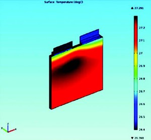
The Thermal Management of Li-ion Battery Packs
At the Fiat Research Center in Italy, Michele Gosso and Antonio Fiumara are working on the development of providing ...
Upgrading the Nuts and Bolts of the Electrical Grid for a New Generation
Migrating the electrical grid to a “smart grid” is usually discussed in terms of IT issues or embedded systems. Yet, ...
Virtually Tuning an Automotive Audio System
HARMAN is a market leader in connected car setups and equips 80% of the world's luxury cars with premium audio ...


