
Besi Improved Memory Chip Manufacturing with Multiphysics Simulation
Stefan Behler, Besi, Switzerland
As memory chips become smaller and smaller, designers must ensure that the chips stay intact during the manufacturing process. Besi develops equipment and assembly processes for substrate and wafer packaging production in markets such as consumer electronics, automotive, industrial, and solar energy. Stefan Behler, a senior expert process engineer, used multiphysics simulation to explore and optimize a new way of peeling off the tape on a memory chip that results in less deformation of the dies. This new method is now used by semiconductor packaging factories all over the world.
Suggested Stories
Powering Offshore Wind Farms with Numerical Modeling of Subsea Cables
Hellenic Cables uses finite element modeling to analyze and validate underground and subsea cable designs for use in ...
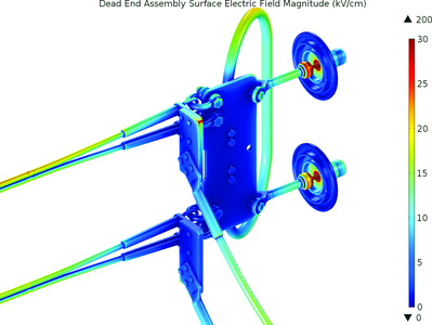
Enhancing Transmission Line Performance: Using Simulation to Optimize Design
Designing power transmission lines requires accounting for many factors: mechanical stress due to environmental ...
Graphene Paves the Way for Next-Generation Plasmonics
Alexander V. Kildishev, associate professor of electrical and computer engineering, is leading computational ...
Illuminating the Physics Behind Electromagnetics Concepts with Applications
Electrical engineering students find it hard to visualize the electromagnetics concepts they are learning. To remedy ...


