Adding a Substrate
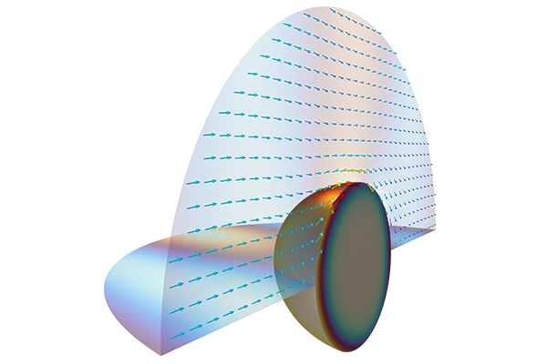
When simulating optical scattering applications using COMSOL Multiphysics® and the Wave Optics Module, you can model complex background geometries along with the corresponding field. You will see a demonstration of this in this article, where we continue to build upon the base application built in the beginning of the course.
Tutorial: Adding a Substrate
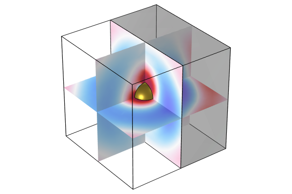
Follow along in the software as we build an example application featuring a typical gold nanosphere on a substrate. Important steps in this process are calculating the background field, applying the calculated field as a user-defined background wave in the physics interface settings, and setting up the study steps. These steps are discussed more following the tutorial.
Calculate the Background Field
After adjusting the geometry and materials section to include a substrate in the form of a block, we need to calculate the background field with a full-field study. For that, we define the following:
- A plane-wave-emitting scattering boundary on the exterior air boundary parallel to the material surface
- An absorbing scattering boundary on the exterior silica boundary parallel to the material surface
- A perfect electric conductor (PEC) symmetry on the exterior boundaries normal to the z-axis
- A perfect magnetic conductor (PMC) symmetry on the exterior boundaries normal to the y-axis
- Two wave equations that replace the gold particle with air and silica, respectively
 A screenshot of the COMSOL Multiphysics user interface, with the Scattering Boundary Condition selected in the Model Builder and a results plot for the background field displayed in the Graphics window.
The Scattering Boundary Condition 1 node settings.
Apply the Calculated Background Field in the Interface for Calculating the Scattering
The calculated background field can now simply be supplied as a user-defined background wave by using the electric field components from the prior Electromagnetic Waves, Frequency Domain interface (ewfd.Ex, ewfd.Ey, ewfd.Ez).
 A screenshot of the COMSOL Desktop, with the second Electromagnetic Waves, Frequency Domain interface selected, the corresponding Settings window, and the results plot of the relative electric field displayed in the Graphics window.
The settings for the second Electromagnetic Waves, Frequency Domain interface added to the model, used to calculate the scattered field.
Setting Up the Study Steps
For this simulation, we need to use two study steps. The first one simulates the background field. The results are automatically passed to the second step, which calculates the scattered fields.
 The Model Builder with a Wavelength Domain study selected and the corresponding Settings window.
The settings for the substrate background field study.
This method can be extended to arbitrary angles of incidence by using the periodic boundaries that take into account the phase of the plane wave, as can be seen in the first model in the Further Learning section below. Furthermore, you can investigate the far field with a substrate, as seen in the second model below.
Further Learning
- Tutorial models:
- Scatterer on Substrate (full angle dependence with periodic boundaries)
- Far-Field Radiation With a Substrate (includes layered backgrounds)
- Multipole Analysis of Electromagnetic Scattering
Submit feedback about this page or contact support here.

